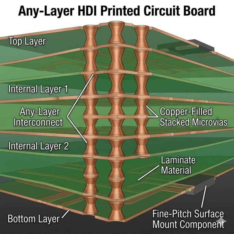
Any-Layer HDI PCB technology, driven by ELIC (Every Layer Interconnection) and stacked microvias, enables the densest interconnects for advanced electronics. This guide explores how these innovations support miniaturization and high-speed performance.
What is an Any-Layer HDI PCB?
Any-Layer HDI PCB allows direct vertical interconnections between any conductive layers using stacked microvias, buried vias, and through-hole vias. Unlike staggered microvias, stacked microvias form a vertical column, eliminating intermediate capture pads and maximizing routing density. This structure supports fine line/space of 50µm or less, high layer counts (8–20+), and sequential lamination cycles for ultra-dense designs.
Key Characteristics of Any-Layer HDI PCB
- High layer count: 8 to 20+ layers.
- Fine line & space: 50µm (2 mils) or less.
- High microvia density: Laser-drilled microvias.
- Sequential lamination: Multiple cycles of lamination and laser drilling.
- Direct interconnection: Any layer to any layer without through-hole vias.
The Core Technology: ELIC (Every Layer Interconnection)
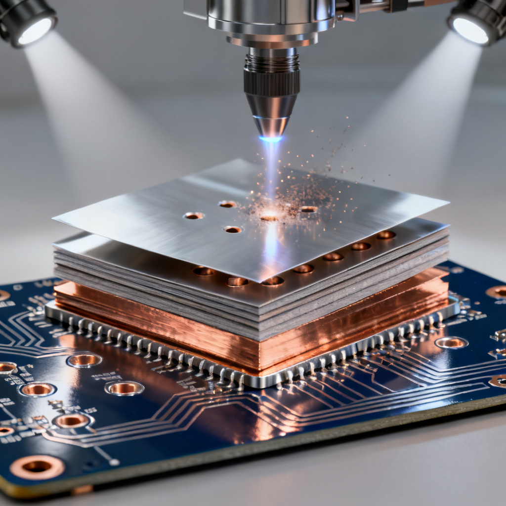
ELIC technology is the proprietary process that makes Any-Layer HDI possible. It involves a repetitive cycle of core formation, lamination, laser drilling, plating, and patterning. Each microvia is drilled directly above the previous layer’s plated via, creating a solid copper column. This method maximizes density, enhances signal integrity by reducing parasitic inductance, and improves reliability under thermal stress.
How ELIC Works
- Core formation: Thin double-sided copper-clad laminate.
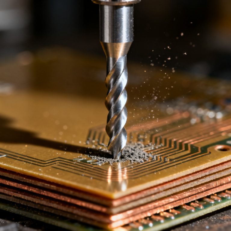
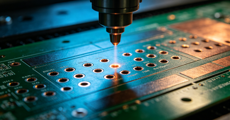
- First lamination & laser drilling: Prepreg and copper foil laminated; CO2 or UV laser drills microvias (60–100µm diameter).
- Plating & patterning: Microvias plated with copper; circuit pattern etched.
- Repetition: Steps 2 and 3 repeated for each layer.
- Final lamination: Outer layers processed.
Why ELIC Matters
- Maximum density: Eliminates capture pads on intermediate layers.
- Superior signal integrity: Shorter paths reduce parasitic effects for high-speed signals (DDR5, PCIe Gen 5/6).
- Enhanced reliability: Solid copper-filled stacked vias resist thermal stress.
- Reduced layer count: Achieves same density with fewer layers, reducing thickness and cost.
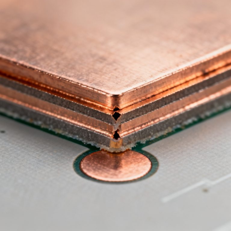
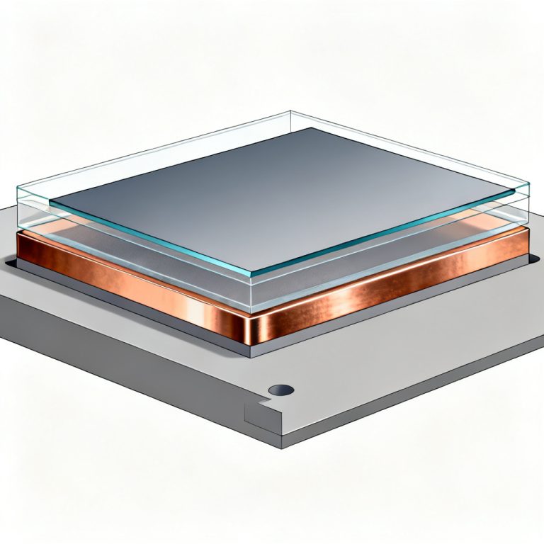
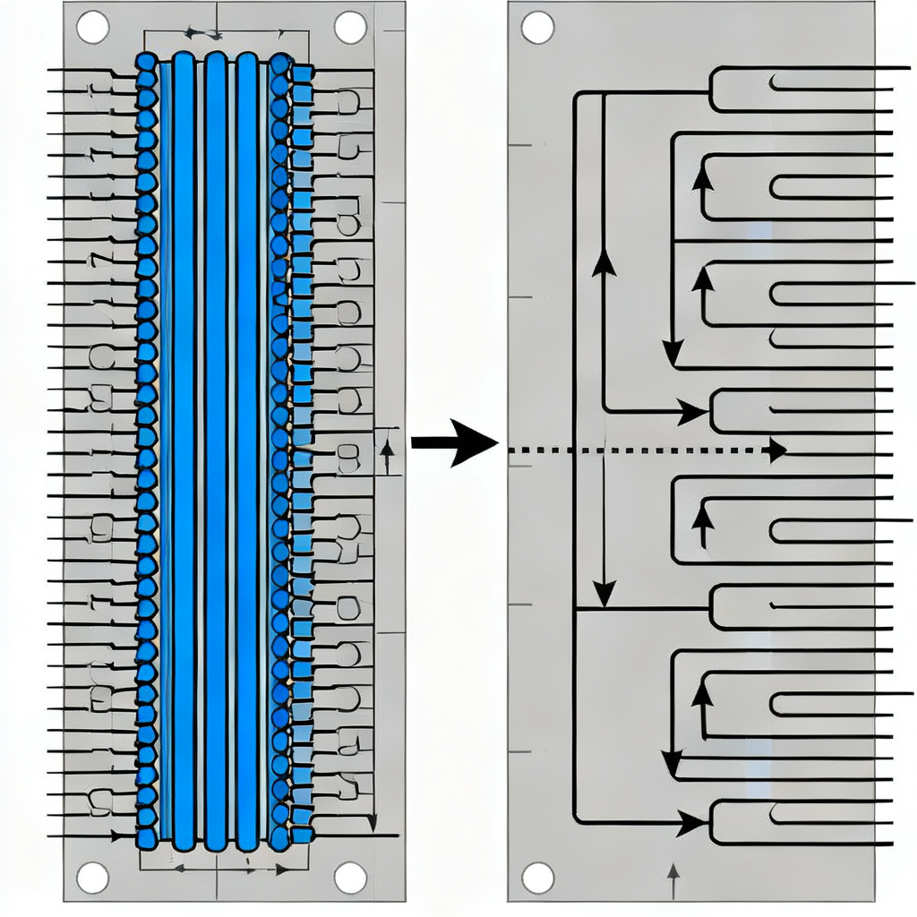
Stacked Microvias: The Building Block
Stacked microvias are vertical columns of plated microvias aligned directly over each other across multiple dielectric layers. This is the fundamental element of Any-Layer HDI PCB.
Comparison: Stacked vs. Staggered Microvias
| Feature | Staggered Microvias | Stacked Microvias |
|---|---|---|
| Alignment | Offset, require capture pads | Vertical, direct connection |
| Routing space | Consumes space | Maximizes routing area |
| Signal path | Longer, more inductive | Shorter, lower inductance |
| Reliability | Prone to via-in-pad issues | Mechanically stronger |
| Typical use | 1+N+1, 2+N+2 HDI | Any-Layer HDI |
Manufacturing Challenges of Stacked Microvias
- Registration accuracy: Tight alignment tolerances (±20µm) for laser drilling.
- Plating uniformity: Consistent copper plating in deep, narrow columns.
- Thermal cycling reliability: CTE mismatch between copper and dielectric; via filling critical.
- Via-in-Pad (VIP) processing: Complete filling and planarization for BGA pads.
Design Considerations for Any-Layer HDI PCB
Designing for Any-Layer HDI PCB requires careful planning. Key considerations include stack-up planning with manufacturers, via structure definition (stacked vs. staggered), pad size optimization, drill-to-copper clearance (75–100µm), impedance control for high-speed signals, and thermal management using stacked thermal vias.
Design Parameters Table
| Parameter | Specification |
|---|---|
| Minimum trace/space | 50µm |
| Microvia diameter | 60–100µm |
| Registration tolerance | ±20µm |
| Drill-to-copper clearance | 75–100µm |
| Layer count range | 8–20+ |
Applications of Any-Layer HDI & ELIC
Any-Layer HDI PCB is indispensable for smartphones, tablets, high-performance computing (HPC), advanced networking (400Gbps+), medical devices, and aerospace/defense. Its ability to handle extreme component density and high-speed signals makes it critical for 5G/6G infrastructure and AI-driven edge devices.
Cost vs. Performance: Is Any-Layer HDI Right for You?
Any-Layer HDI PCB is the most expensive PCB technology due to multiple sequential laminations, tight tolerances, yield loss, and high-performance materials (e.g., Megtron 6, R-1755S). Choose it for extreme component density (0.4mm pitch BGA), direct via-in-pad connections, paramount signal integrity, or critical thickness constraints. For moderate density (1+N+1 or 2+N+2 HDI), staggered microvias are more cost-effective.
FAQ: Any-Layer HDI PCB, ELIC & Stacked Microvias
What is the difference between Any-Layer HDI and standard HDI?
Standard HDI uses staggered microvias, while Any-Layer HDI uses stacked microvias for direct layer-to-layer connections, offering higher density and better signal integrity.
How does ELIC technology improve PCB reliability?
ELIC creates solid copper-filled stacked vias that resist thermal stress and mechanical failure, enhancing reliability in high-performance applications.
What are the key challenges in manufacturing stacked microvias?
Challenges include registration accuracy, plating uniformity, thermal cycling reliability, and via-in-pad processing.
Is Any-Layer HDI suitable for high-speed digital designs?
Yes, Any-Layer HDI PCB is ideal for high-speed signals like DDR5 and PCIe Gen 5/6 due to reduced parasitic effects and controlled impedance.
What materials are commonly used for Any-Layer HDI?
High-performance materials like Megtron 6, R-1755S, and low-loss laminates are used to meet signal integrity and thermal requirements.
Conclusion: The Future of PCB Interconnection
Any-Layer HDI PCB, powered by ELIC technology and stacked microvias, represents the pinnacle of miniaturization and performance. While costly, it enables next-generation electronics. Understanding this technology is essential for competitive product design.