HDI & Ultra-HDI PCBs represent a fundamental shift in printed circuit board fabrication. This any-layer high density interconnect guide addresses the manufacturing realities, design constraints, and high-reliability production requirements for next-generation electronics.
Market Context for HDI & Ultra-HDI PCBs
The transition to Ultra-HDI PCBs is driven by economic and legislative forces. The global shift toward semiconductor sovereignty and advanced packaging places any-layer high density interconnect technology at the center of industrial policy. The U.S. CHIPS and Science Act explicitly identifies advanced substrates and high-density PCBs as critical supply chain components, accelerating investment in domestic UHDI capacity.
The market for Ultra-HDI PCBs is projected to grow at a compound annual growth rate (CAGR) significantly outpacing standard rigid PCBs. This growth is fueled by heterogeneous integration, escalating power density requirements, and the need to maintain signal integrity at frequencies exceeding 10 GHz. For B2B buyers, selecting a HDI & Ultra-HDI PCBs partner is now a strategic risk management decision tied directly to product performance and time-to-market.
Defining HDI & Ultra-HDI PCBs: Technology Comparison
While standard HDI is defined by microvias and sequential lamination, Ultra-HDI PCBs are defined by sub-25-micron trace and space capabilities. The following table provides a definitive comparison of key technical parameters that distinguish these fabrication classes.
| Parameter | Standard PCB | Advanced HDI (Any-Layer) | Ultra-HDI PCBs |
|---|---|---|---|
| Min. Trace/Space | 75 µm / 75 µm | 40 µm / 40 µm | < 25 µm / < 25 µm |
| Min. Microvia Diameter | 100 µm | 75 µm | < 50 µm |
| Dielectric Thickness | > 60 µm | 40-60 µm | < 30 µm |
| Primary Patterning Process | Subtractive Etch | Modified Semi-Additive (mSAP) | Semi-Additive (SAP) / Advanced mSAP |
| Typical Layer Count | 4-12 | 8-20 | 10-30+ |
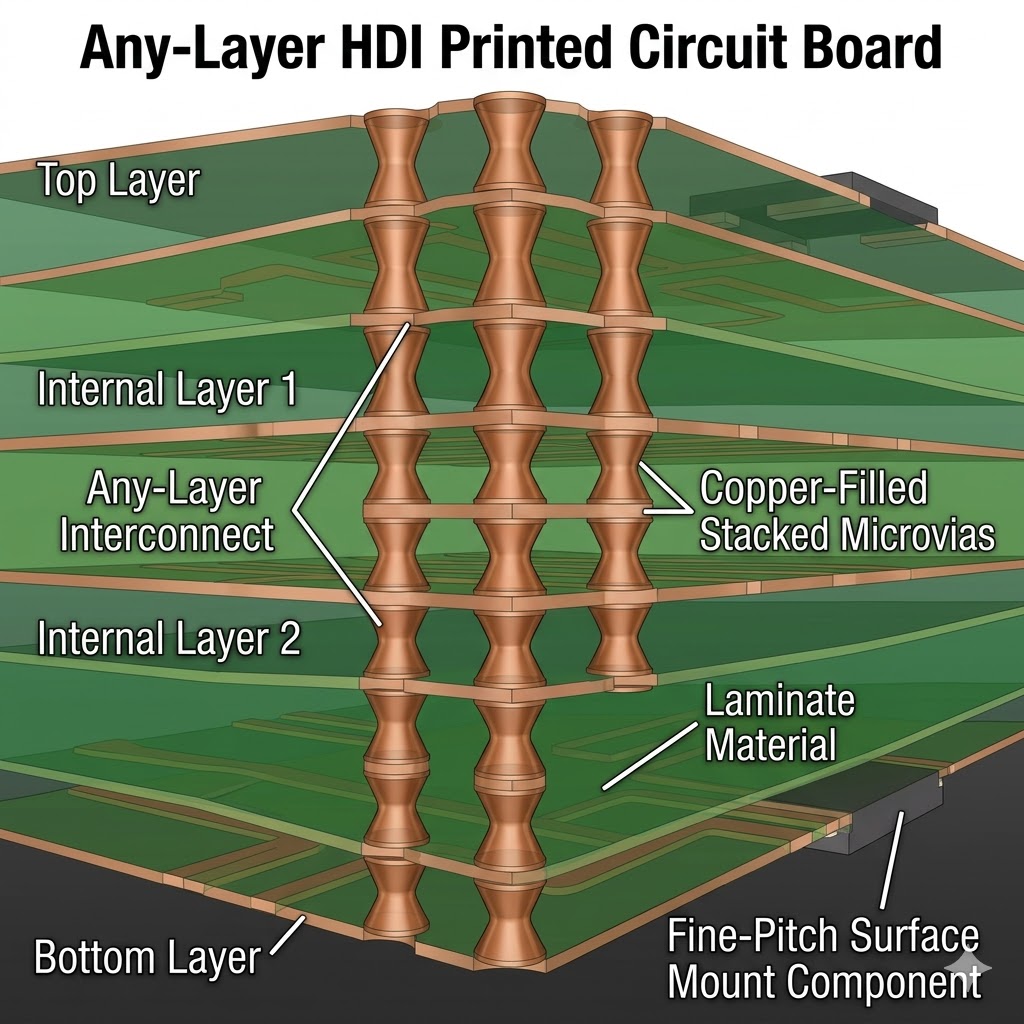
What is Any-Layer HDI (Every Layer Interconnect)?
Any-layer HDI refers to a construction where every single layer in the stackup is a microvia layer. Unlike sequential lamination builds (1+N+1, 2+N+2), any-layer high density interconnect uses copper-filled stacked microvias to connect directly from the top layer to any internal layer or to the bottom layer without mechanical through-holes. This eliminates stub resonance and maximizes routing density, making it the preferred architecture for high-speed digital and RF applications.
The Ultra-HDI Distinction
Moving into the Ultra-HDI PCBs space introduces “a wholly distinct operational paradigm.” At these dimensions, the glass weave effect of standard FR-4 becomes a dominant yield limiter, and traditional laser drilling parameters must be recalibrated for extremely thin copper foils. This is a core consideration for any HDI & Ultra-HDI PCBs manufacturing partner.
Core Manufacturing Technologies for Ultra-HDI PCBs
Achieving reliable, high-volume production of any-layer high density interconnect boards requires mastery over three interdependent process technologies. The following sections detail the technical realities designers must consider to ensure manufacturability at scale.
The Shift to Semi-Additive Processing (SAP and mSAP)
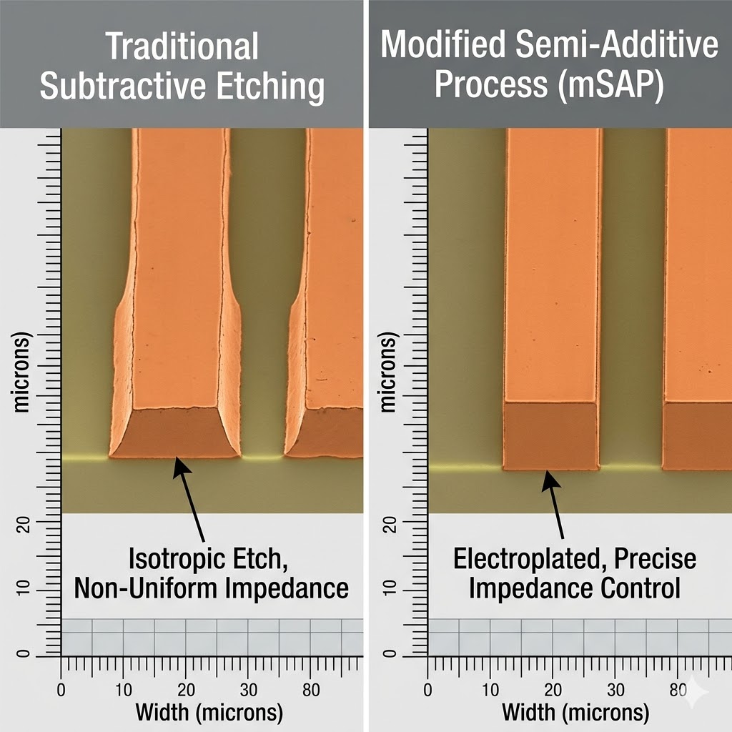
The most significant process change in Ultra-HDI PCBs is the departure from Subtractive Etching. When trace widths drop below 30 µm, the isotropic nature of the etchant creates trapezoidal cross-sections that violate impedance control requirements and risk trace lifting. In subtractive etching, the etch solution attacks copper laterally under the resist; for a 20 µm trace, the etch factor becomes uncontrollable. The UHDI solution is Modified Semi-Additive Process (mSAP) or full Semi-Additive Process (SAP). In this workflow, a thin seed layer of copper is plated onto the laminate. A resist pattern is applied, and the circuit traces are plated up electrochemically. The resist is then stripped, and the unwanted seed layer is flash-etched away quickly. This process produces nearly vertical sidewalls (rectangular traces), which drastically improves signal integrity and fine-pitch routing density in HDI & Ultra-HDI PCBs.
Laser Drilling and Stacked Microvia Reliability
Any-layer HDI relies on Stacked Copper-Filled Microvias. The reliability of these structures is paramount. As microvia diameters shrink toward 40-50 µm, the aspect ratio (depth/diameter) must be managed. Shallow, wide vias are preferred over deep, narrow ones. At UHDI dimensions, the fiberglass weave in the laminate becomes a major issue. A 30 µm dielectric thickness may only contain a single layer of glass fibers. If the laser hits a glass bundle versus a resin pocket, the hole quality varies significantly. This necessitates the use of spread glass or ultra-thin homogenous dielectrics (e.g., Ajinomoto Build-up Film). Via-in-Pad (VIPPO) is mandatory for dense BGA breakout in HDI & Ultra-HDI PCBs. For a 0.35 mm pitch BGA, the target pad must be precisely controlled; over-plating or dimpling in the pad surface can lead to solder joint voids and intermittent opens.
Layer-to-Layer Registration
In a 20-layer any-layer high density interconnect board, the accumulated registration tolerance between the first and last layer can exceed the width of the trace itself if not managed with precision. If each lamination step introduces a ±10 µm shift, and the board undergoes 4 lamination cycles, the total shift could be 40 µm. For a 25 µm trace, this results in a 160% misalignment. High-yield Ultra-HDI PCBs fabrication requires X-ray drilling to locate internal targets for outer layer alignment, effectively “zeroing out” the cumulative lamination drift. This process, while critical, adds cycle time to the fabrication flow.
Design for Manufacturing (DFM) for HDI & Ultra-HDI PCBs
A design that works in a simulation environment may fail catastrophically on the fab floor. The following constraints, derived from deep collaboration between designers and manufacturing engineers, are non-negotiable for Ultra-HDI PCBs success.
Material Selection: Beyond Standard FR-4
The standard 106 or 1080 prepregs used in standard HDI are often too thick and non-uniform for UHDI. The design must specify materials that balance Dk (Dielectric Constant) stability with CAF (Conductive Anodic Filament) resistance. Low-profile copper foils (HVLP) paired with low-Dk, low-loss laminates (Megtron 6, Tachyon-100G, or specialized BT resins) are recommended. These materials minimize signal attenuation and reduce the risk of skew in differential pairs within any-layer high density interconnect stackups.
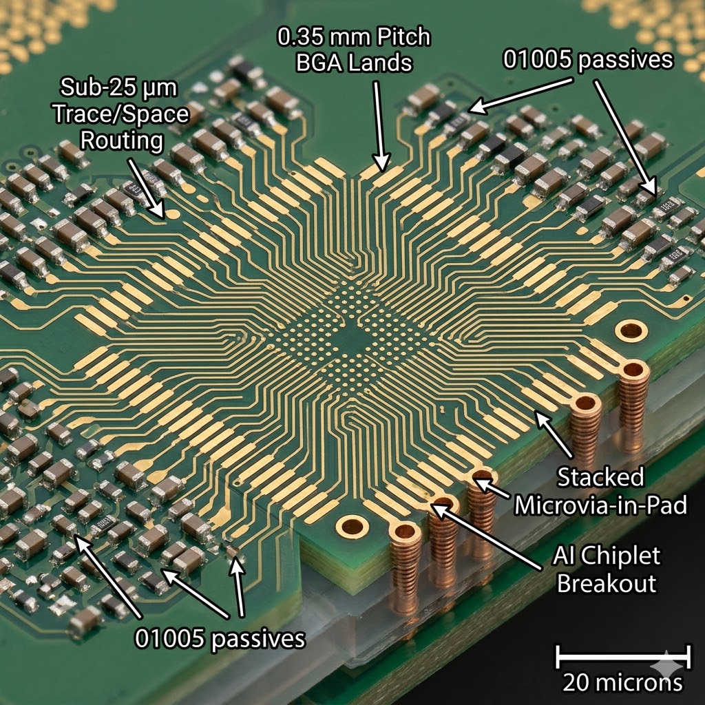
The Reality of Fan-Out for Fine-Pitch Devices
The most illustrative example of Ultra-HDI PCBs necessity comes from modern semiconductor packaging. Consider the challenge of routing a 0.35 mm pitch BGA for an AI accelerator. BGA Ball Pitch is 0.35 mm (350 µm); Ball Diameter is ~200 µm; Space between adjacent pads is 350 µm – 200 µm = 150 µm. To route one single trace between two pads, the clearance rule demands roughly: Trace Width 20 µm, Air Gap 20 µm (left) + 20 µm (right) = 40 µm, total width consumed 60 µm. Using Ultra-HDI PCBs rules (20/20 µm trace/space), you can route two traces between BGA pads or one trace with a via pad. Using standard HDI rules (50/50 µm), you route zero traces. Ultra-HDI PCBs are not an option for these packages; they are the only path to connectivity.
Via Stacking Strategy
Designers often stack microvias to the maximum extent to save space in any-layer HDI designs. While possible, it is prudent to stagger vias on at least one internal layer if the board thickness exceeds 1.6 mm. Stacked vias act as rigid copper columns; during reflow or thermal cycling, the Z-axis expansion mismatch between the copper column and the laminate can induce latent cracks at the bottom of the stack in HDI & Ultra-HDI PCBs.
Architecting Ultra-HDI PCBs for AI, Chiplets, and Fan-Out Packaging
The most demanding application driving Ultra-HDI PCBs adoption is the AI/ML Acceleration Cluster. As described in advanced engineering forums, the architecture of these boards has evolved into a discipline of its own—Architecting HDI for Ultra-Fine-Pitch Chiplets.
Breaking Out the Chiplet Ecosystem
Modern AI processors (GPUs and custom ASICs) are increasingly adopting Chiplet architectures. Instead of one monolithic die, the package contains multiple smaller dies (compute, memory I/O, SRAM) connected via high-speed interfaces like Universal Chiplet Interconnect Express (UCIe). The board-level substrate must act as a seamless extension of the package. It must manage ultra-wide parallel buses (1024-bit HBM interfaces) and extremely low latency. Any-layer HDI allows the designer to minimize via stub lengths to near zero, preserving signal eye height at 32 GT/s and beyond in HDI & Ultra-HDI PCBs.
Power Integrity in Ultra-Dense Routing
As voltage rails drop below 0.8V to save power in AI chips, current demands skyrocket (often exceeding 500A for a single socket). This creates a Power Delivery Network (PDN) Paradox: You need wide copper shapes for power, but Ultra-HDI PCBs use thin copper foils and fine traces. The solution necessitates the use of Embedded Copper Coins or Thick Copper Core Layers sandwiched within the UHDI build-up layers. This hybrid construction allows for 2 oz (70 µm) power planes in the center while maintaining 15 µm trace geometry on the surface layers for signal escape.
Thermal Management of High-Density Interconnect
HDI & Ultra-HDI PCBs are dense in both electrical routing and thermal energy. The fine lines and thin dielectrics have higher thermal resistance than standard FR-4 boards. Heat generated by the BGA chip must travel vertically down through stacked copper vias. If the via stack is not designed with a direct thermal path to an internal ground plane or external heatsink, the junction temperature will exceed reliability limits. We recommend thermally aware DFM analysis during the quotation stage to identify potential hot spots before production begins.
High-Volume Yield Challenges for Ultra-HDI PCBs
The final frontier of any-layer high density interconnect is scaling from prototype to volume production. While a lab can produce a single perfect 5-mil trace, a production line must produce millions of them with zero defects.
Surface Finish Uniformity
Standard ENIG (Electroless Nickel Immersion Gold) can create a “Black Pad” risk on ultra-fine pads due to nickel corrosion. For Ultra-HDI PCBs applications, Electroless Palladium Immersion Gold (EPIG) or Immersion Silver are preferred due to their flatter topography and suitability for wire bonding on adjacent chiplet footprints.
Solder Mask Registration and Clearance
The solder mask dam between two 25 µm traces is often less than 40 µm. Inkjet legend or Laser Direct Imaging (LDI) for solder mask is mandatory to prevent mask encroachment onto surface mount pads, which would cause tombstoning of 01005 (0.4mm x 0.2mm) passive components on HDI & Ultra-HDI PCBs.
The Knowledge Gap: Communication is Key
As noted by the engineering community, the most significant risk factor in UHDI projects is the gap between design intent and fab floor reality. A designer might spec a 15 µm trace, but if they do not specify copper roughness (Rz) or surface treatment thickness, the final impedance will be off-target.
Future Trends in HDI & Ultra-HDI PCBs
Looking forward, the lines between PCB, substrate, and semiconductor packaging will continue to blur. Glass core substrates are emerging to overcome the CTE mismatch of organic laminates, offering near-zero warpage and ultra-flat surfaces for sub-5 µm line/space patterning. Embedded active components represent the next step—embedding bare silicon dies inside the PCB layers (Embedded Component Packaging), which will require even tighter cavity tolerances and laser drilling precision for Ultra-HDI PCBs. Digital twin fabrication is moving toward a model where the entire manufacturing process is simulated digitally before a single sheet of laminate is cut, predicting yield based on Gerber data and material batch properties.
Partnering for HDI & Ultra-HDI PCBs Success
Navigating the transition from standard HDI to any-layer high density interconnect requires more than a supplier; it requires a fabrication partner who understands the intersection of physics, materials science, and volume economics. At [Your Company Name], our manufacturing infrastructure is purpose-built for the Ultra-HDI PCBs paradigm. We combine advanced mSAP processing lines, high-precision laser direct imaging, and a rigorous DFM engineering team that reviews every design through the lens of high-yield, high-reliability production. Whether you are scaling an AI inference board, designing a ruggedized RF module for defense, or pushing the boundaries of miniaturized medical wearables, our capabilities in stacked microvias, fine-line etching (<2 mil), and advanced material handling ensure your next-generation product reaches the market with the performance and reliability your customers demand.
Frequently Asked Questions About HDI & Ultra-HDI PCBs
What is the difference between HDI and Ultra-HDI PCBs?
Standard HDI typically features trace/space of 40 µm or larger, while Ultra-HDI PCBs achieve trace/space below 25 µm. The manufacturing process shifts from subtractive etching to semi-additive processing (mSAP/SAP), enabling any-layer high density interconnect for advanced semiconductor packaging.
What are the primary applications for any-layer HDI PCBs?
Any-layer HDI is essential for AI accelerators, chiplet-based processors, 5G/6G infrastructure, ADAS automotive systems, and high-end medical devices. These applications demand the routing density and signal integrity that only Ultra-HDI PCBs can provide.
Why is mSAP required for Ultra-HDI PCBs manufacturing?
At trace widths below 30 µm, traditional subtractive etching creates trapezoidal traces that compromise impedance control. mSAP (Modified Semi-Additive Process) plates traces upward from a thin seed layer, producing vertical sidewalls essential for HDI & Ultra-HDI PCBs performance and reliability.
What materials are recommended for Ultra-HDI PCBs?
Ultra-HDI PCBs require low-profile copper foils (HVLP) paired with low-Dk, low-loss laminates such as Megtron 6, Tachyon-100G, or specialized BT resins. Spread glass or homogenous build-up films are necessary to manage laser drilling consistency in thin dielectrics.
How do you ensure high-volume yield for HDI & Ultra-HDI PCBs?
High-yield production of HDI & Ultra-HDI PCBs requires X-ray registration systems, laser direct imaging (LDI) for solder mask, and rigorous control of surface finish uniformity. A strong DFM partnership between designer and fabricator is critical to bridge the gap between design intent and fab floor reality.