In the rapidly evolving world of electronics, demand for smaller, faster, and more reliable printed circuit boards (PCBs) is relentless. From 5G telecommunications and high-performance computing (HPC) to automotive ADAS and medical devices, complexity requires advanced PCB manufacturing techniques. This pillar page covers three critical technologies: laser drilling, Modified Semi-Additive Process (mSAP), and backdrilling. These processes are essential for achieving higher density interconnects (HDI), finer trace widths, and superior signal integrity. If you are a B2B buyer or engineer seeking high-quality, reliable PCBs, understanding these technologies is paramount.
Laser Drilling – The Foundation of HDI PCBs (Advanced PCB Manufacturing)
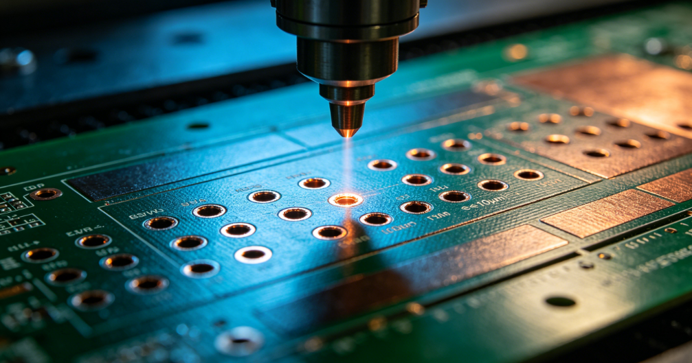
Laser drilling has revolutionized multi-layer PCB interconnections. Traditional mechanical drilling cannot achieve precision required for microvias—small holes with diameters typically less than 150 micrometers (µm). Laser drilling is the cornerstone of HDI technology.
1.1 What is Laser Drilling? (Advanced PCB Manufacturing)
Laser drilling uses a focused beam of light to vaporize dielectric material (prepreg or resin-coated copper) to create a hole. Two primary laser types are used:
- CO2 Lasers: Excellent for removing organic dielectric materials (e.g., FR-4, polyimide) but cannot cut copper directly. Efficient for larger vias (100-200 µm).
- UV Lasers: Capable of cutting through both copper and dielectric. Offer higher precision (down to 25-50 µm) for small vias, blind vias, and staggered vias.
1.2 Key Techniques: Blind, Buried, and Stacked Vias (Advanced PCB Manufacturing)
Laser drilling enables several via structures critical for HDI:
- Blind Vias: Connect outer layer to inner layer, ending at specific depth.
- Buried Vias: Connect two or more inner layers without reaching outer layers.
- Stacked Vias: Multiple vias stacked directly on top of each other, requiring via filling.
- Staggered Vias: Vias offset in stair-step pattern.
1.3 Process Flow for Laser-Drilled Microvias (Advanced PCB Manufacturing)
- Layer Preparation: Inner layers etched, copper foil laminated.
- Laser Ablation: Laser scans panel, creating via holes.
- Desmearing: Chemical or plasma process removes residual resin.
- Electroless Copper Deposition: Thin copper layer on hole walls.
- Electrolytic Copper Plating: Vias plated to required thickness.
- Via Filling: Microvias filled with copper for planar surface.
1.4 Materials and Limitations (Advanced PCB Manufacturing)
Laser drilling is effective on materials like FR-4, high-speed laminates (Rogers, Isola), and polyimide. Challenges include copper thickness, glass weave, and depth control.
1.5 Why It Matters for Your Design (Advanced PCB Manufacturing)
Laser drilling enables higher density, reduced layer count, and improved signal integrity.
mSAP – Enabling Ultra-Fine Traces (Advanced PCB Manufacturing)
As component pitches shrink below 0.4 mm, traditional subtractive etching becomes impractical. The Modified Semi-Additive Process (mSAP) is the breakthrough for trace widths down to 30 µm.
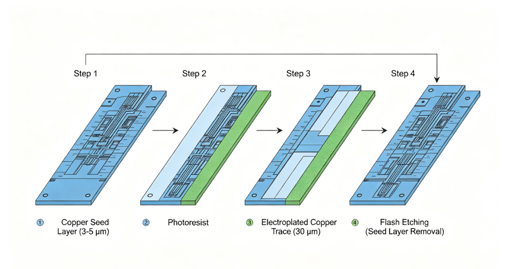
2.1 What is mSAP? (Advanced PCB Manufacturing)
mSAP is a hybrid process combining subtractive and additive manufacturing. Unlike traditional etching, mSAP builds copper only where needed, resulting in finer features.
2.2 The mSAP Process Step-by-Step (Advanced PCB Manufacturing)
- Lamination: Thin copper foil (3-5 µm) laminated onto substrate.
- Photo-Resist Application: Dry film photoresist applied and exposed.
- Electrolytic Copper Plating: Copper plated in exposed areas.
- Resist Stripping: Photoresist removed.
- Flash Etching: Thin seed layer etched away quickly.
2.3 Advantages Over Traditional Etching (Advanced PCB Manufacturing)
| Feature | Traditional Etching (Subtractive) | mSAP (Modified Semi-Additive) |
|---|---|---|
| Minimum Trace Width | 75-100 µm | 25-50 µm |
| Copper Thickness | Defined by starting foil | Controlled by plating |
| Undercut | Significant | Minimal |
| Aspect Ratio | Limited | Excellent |
| Cost | Lower for standard designs | Higher for fine-line designs |
| Best For | Standard PCBs | HDI, IC substrates |
2.4 Materials and Design Considerations for mSAP (Advanced PCB Manufacturing)
Requires ultra-smooth copper foil (HVLP) and low-loss dielectrics (ISOLA, Rogers, Panasonic Megtron). Design rules: trace width/space 30/30 µm or finer, reduced pad size, via-in-pad support.
2.5 Why mSAP is Critical for Advanced PCBs (Advanced PCB Manufacturing)
Enables miniaturization, higher routing density, improved electrical performance, and support for advanced packages.
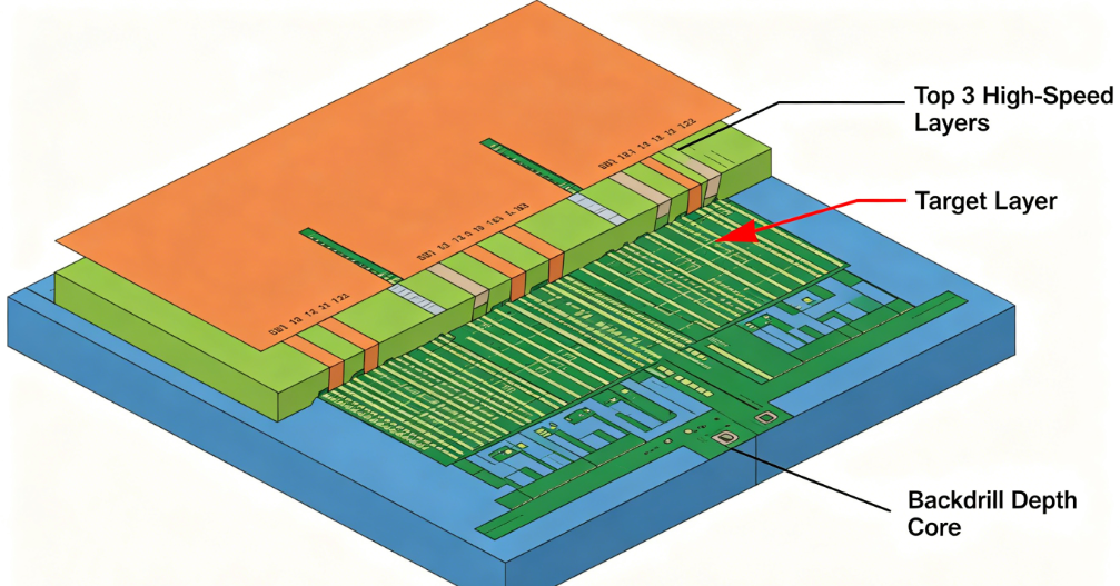
Backdrilling – Eliminating Via Stubs for Signal Integrity (Advanced PCB Manufacturing)
In high-speed digital designs (10 Gbps+), via stubs cause signal reflections and jitter. Backdrilling removes these stubs.
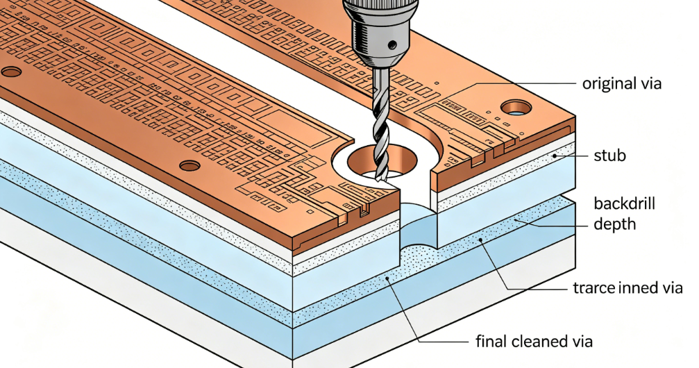
3.1 What is Backdrilling? (Advanced PCB Manufacturing)
Backdrilling is a controlled-depth drilling operation removing copper plating from unused via portions, leaving only electrically needed sections.
3.2 The Backdrilling Process (Advanced PCB Manufacturing)
- Initial Drilling and Plating: PCBs manufactured with through-hole vias.
- Backdrill Operation: Specialized machine drills from opposite side.
- Deburring and Cleaning: Hole cleaned of debris.
- Plugging (Optional): Hole plugged with epoxy or solder mask.
3.3 Key Parameters for Backdrilling (Advanced PCB Manufacturing)
Drill depth tolerance ±0.1 to ±0.2 mm, aspect ratio 10:1 or lower, drill bit diameter 0.1 mm larger than via, stub length less than 0.5 mm (20 mils) for 10 Gbps.
3.4 When is Backdrilling Required? (Advanced PCB Manufacturing)
Required for high-speed serial links (PCIe Gen 3/4/5, USB 3.0/3.1), gigabit Ethernet, memory interfaces (DDR3/DDR4/DDR5), RF designs, and backplane/midplane designs.
3.5 Benefits of Backdrilling (Advanced PCB Manufacturing)
Reduced insertion loss, lower return loss, reduced jitter, improved SNR.
3.6 Design Guidelines for Backdrilling (Advanced PCB Manufacturing)
Place high-speed layers close to top/bottom, maintain 0.5 mm clearance between vias, specify starting/ending layers, avoid copper pours above/below backdrilled area.
Synergy of Technologies – A Case for Advanced Manufacturing (Advanced PCB Manufacturing)
These technologies work together. Example: A 20-layer HDI board for 5G base stations uses laser drilling for microvias, mSAP for 30/30 µm traces, and backdrilling for via stubs.
4.1 Choosing the Right Partner (Advanced PCB Manufacturing)
Look for certifications (ISO 9001, IATF 16949, AS9100, IPC Class 3), advanced equipment, engineering support, and testing capabilities.
4.2 Cost and Lead Time Considerations (Advanced PCB Manufacturing)
Laser drilling adds cost per panel and 2-5 days lead time. mSAP is 2-3x higher cost with 10-15 days lead time. Backdrilling adds $50-$200 per board and 3-7 days lead time.
Conclusion (Advanced PCB Manufacturing)
Advanced PCB manufacturing is a necessity for modern electronics. Laser drilling enables microvias for HDI, mSAP allows ultra-fine traces, and backdrilling ensures signal integrity. At [Your Company Name], we specialize in these advanced processes. Contact our engineering team for a DFM review and quote.
FAQ: Advanced PCB Manufacturing with Laser Drilling, mSAP & Backdrill
What is the difference between laser drilling and mechanical drilling in advanced PCB manufacturing?
Laser drilling uses focused light to create microvias (<150 µm) essential for HDI, while mechanical drilling is limited to larger holes (>200 µm).
How does mSAP improve advanced PCB manufacturing for high-density designs?
mSAP enables trace widths down to 30 µm, supporting miniaturization and higher routing density for advanced PCB manufacturing.