Backdrilling PCB is a critical manufacturing process that removes unused via stubs from through-hole vias, directly addressing signal integrity issues in high-speed digital and RF designs. This guide provides a complete engineering-level overview of backdrilling, including why it is necessary, how it works, design rules, manufacturing constraints, and how to specify it correctly for your next high-speed PCB.
1. What is a Via Stub? The Root Cause of Signal Degradation
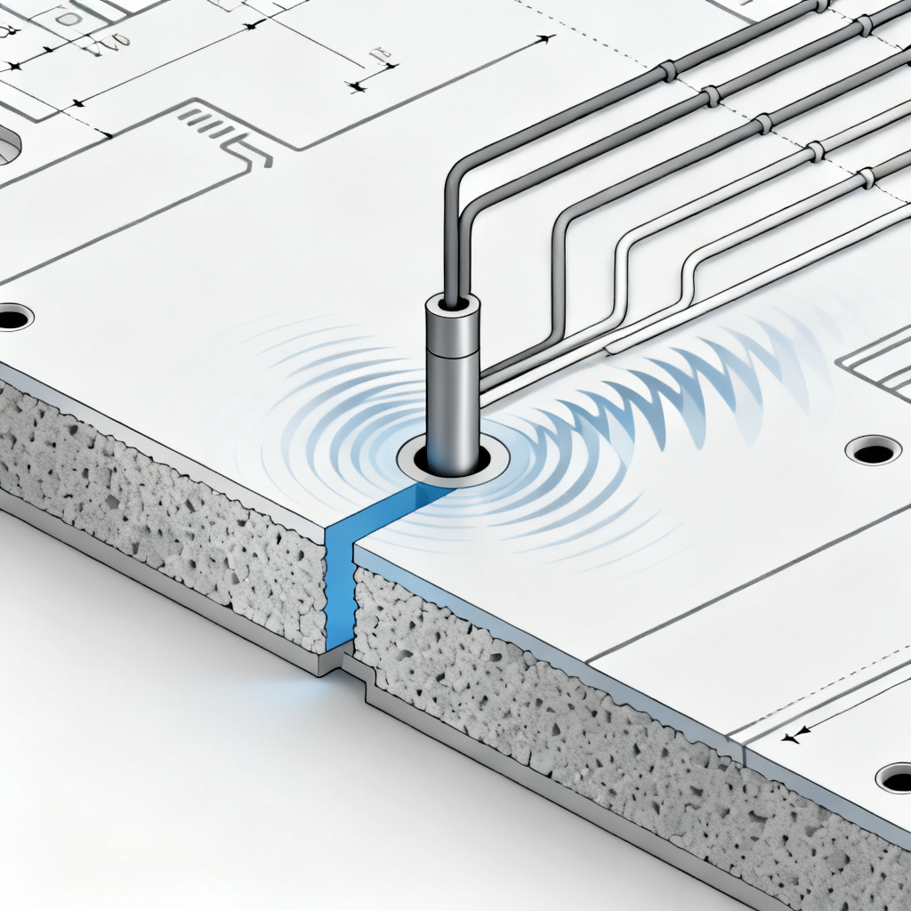
A via stub is essentially a short, open-ended transmission line stub attached to your signal path. It is created because standard PCB fabrication uses through-hole vias that drill through the entire board thickness, even when the signal only travels between a few inner layers. This stub acts as a resonator at high frequencies, causing reflections, insertion loss, and impedance discontinuities.
1.1 The Physics of the Stub
The stub length determines its resonant frequency. A quarter-wavelength stub acts as an open circuit, while a half-wavelength stub acts as a short circuit. The stub resonates at frequencies where its length is an odd multiple of a quarter-wavelength. Even before resonance, the stub introduces parasitic capacitance, lowering the impedance of the via and causing reflections. This creates a notch filter effect, causing significant signal loss at specific frequencies, often visible in S-parameter measurements (S21) as a deep dip at the stub’s resonant frequency.
1.2 When Does a Stub Become a Problem?
If the stub length exceeds 10% of the signal’s rise time distance, it will cause measurable signal degradation. For signals above 1 Gbps or with rise times less than 1 ns, via stubs longer than 10-15 mils (0.25-0.38 mm) should be removed. Critical applications include high-speed serial interfaces (PCIe Gen 4/5, USB 3.x, HDMI 2.1, 10/25/40/100 GbE), RF/microwave circuits (above 1 GHz), and DDR memory interfaces (DDR4/5).
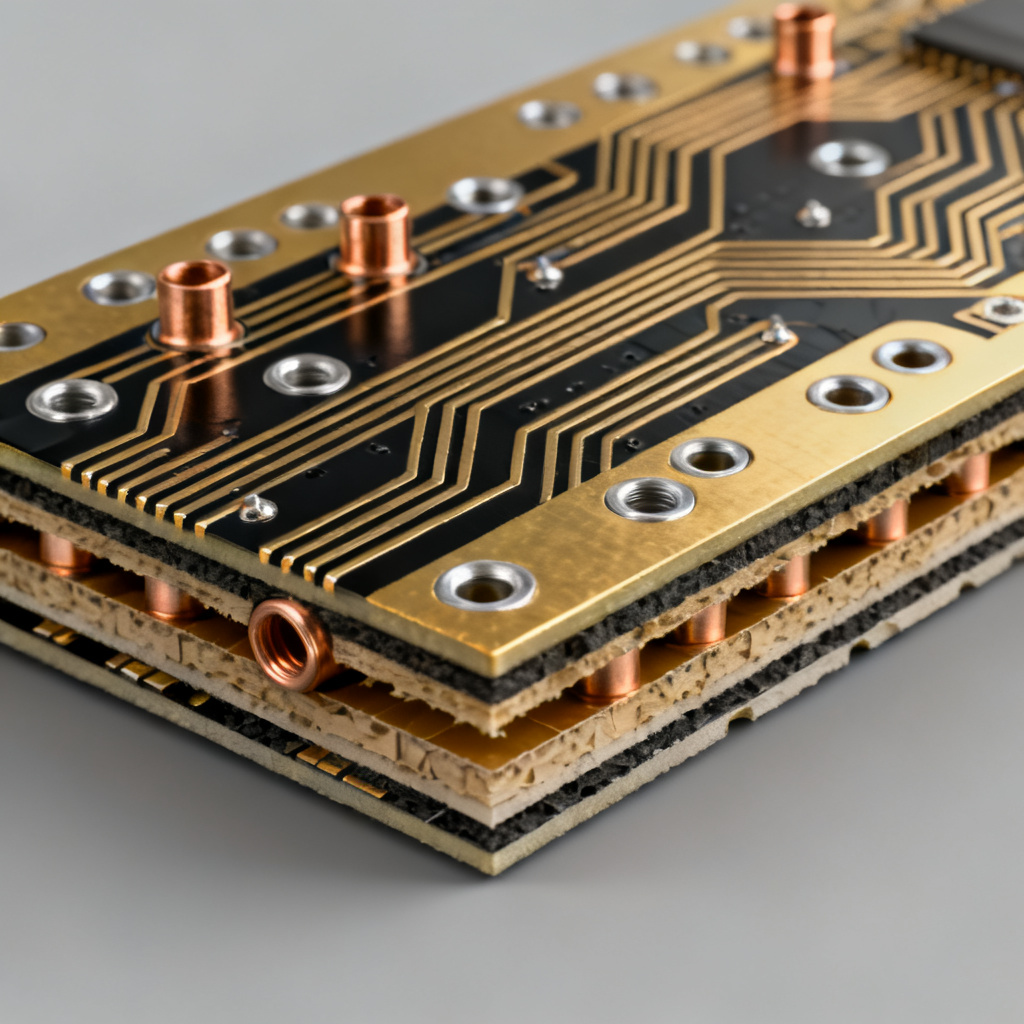
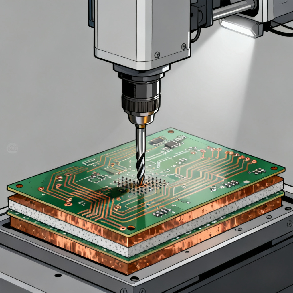
2. How Backdrilling Works: The Manufacturing Process
Backdrilling is a secondary mechanical drilling operation performed after the standard PCB lamination, plating, and etching are complete. It is not a replacement for standard via drilling.
2.1 Step-by-Step Process
First, the PCB is manufactured normally, including drilling of all through-hole vias, copper plating, and outer layer patterning. Then, a specialized backdrilling machine uses a larger drill bit (typically 0.3 mm to 1.0 mm larger than the original via diameter) to drill from the surface of the board down to a specific depth. This depth is precisely calculated to stop just below the target signal layer, removing the copper barrel of the unused portion. The backdrilled holes are then cleaned to remove copper debris, epoxy smear, and drill burrs. Finally, X-ray inspection or automated optical inspection (AOI) is used to verify the backdrill depth and alignment.
2.2 Key Terms
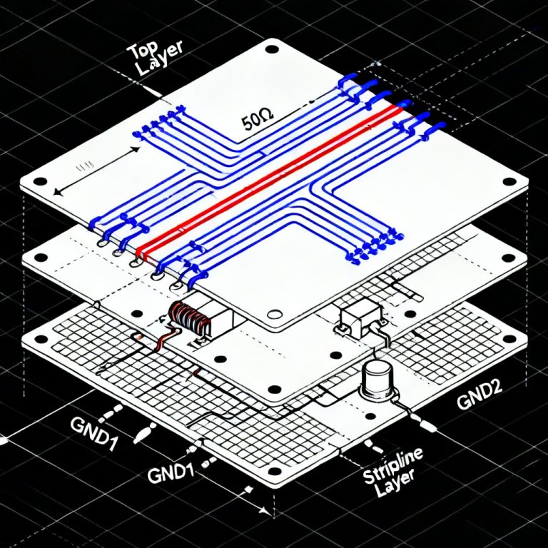
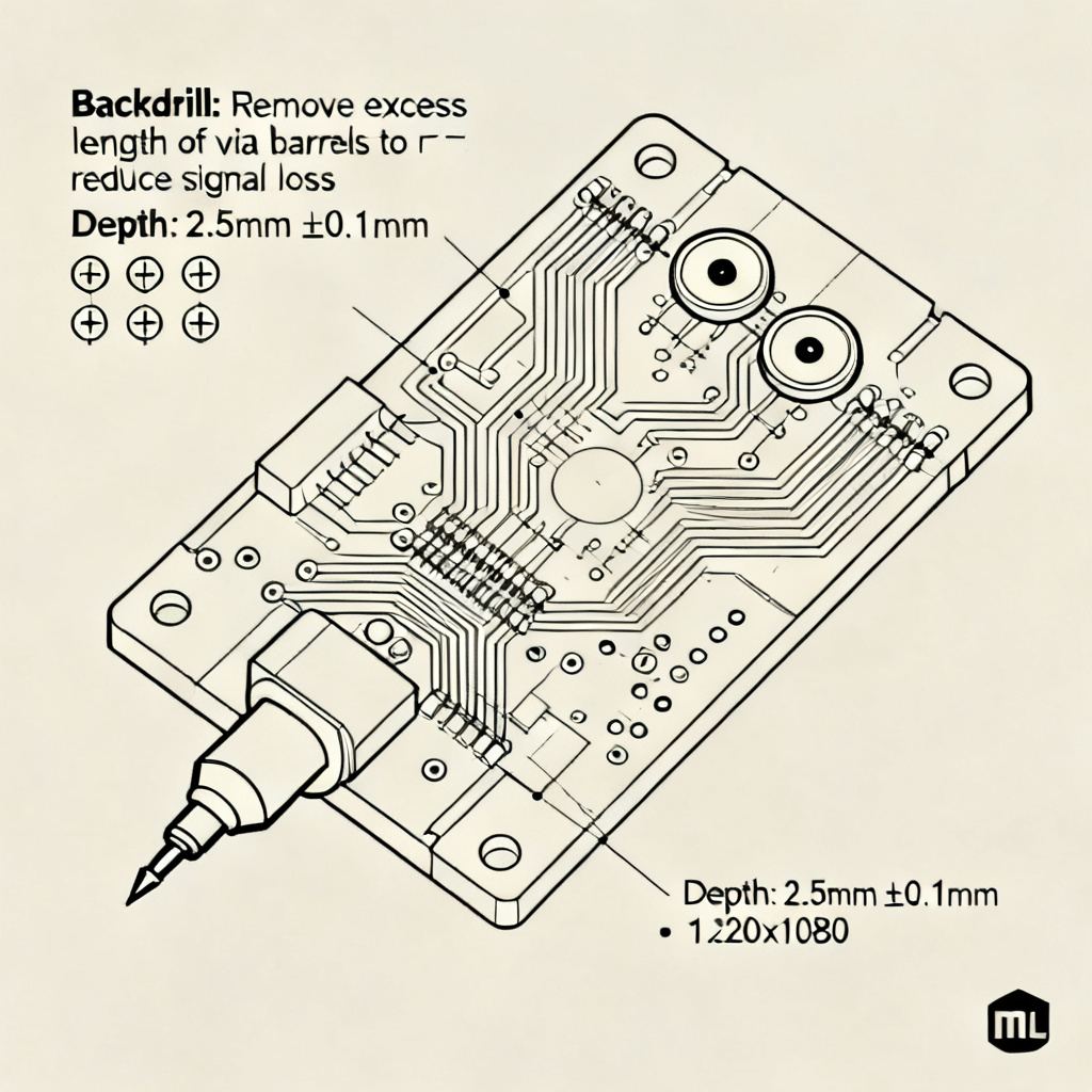
Stub Length is the remaining copper barrel after backdrilling, with the goal to minimize this to <10 mils (0.25 mm). Backdrill Depth is the depth to which the drill penetrates the board, typically specified from the top or bottom surface. The Drill Bit Diameter must be larger than the original via to ensure complete removal of the copper plating. Backdrill Layer refers to the layer from which the backdrilling is performed (e.g., “Backdrill from Layer 1 to Layer 3”).
3. Design Rules and Constraints for Backdrilling
To ensure manufacturability and optimal performance, designers must follow specific rules.
3.1 Aspect Ratio Limits
Backdrilling has a maximum depth-to-diameter ratio, commonly 8:1 to 12:1. For example, a 0.5 mm drill bit can backdrill up to 4-6 mm deep. Exceeding this risks drill breakage and poor hole quality. For thick boards (e.g., 3.2 mm or 0.125 inch), backdrilling from both sides may be required to keep the aspect ratio within limits.
3.2 Clearance and Annular Ring Requirements
The backdrill bit must have a minimum 5 mil (0.127 mm) clearance from any remaining copper features on the layers it passes through. The backdrill bit is typically 0.3 mm to 1.0 mm larger than the original via diameter. Surrounding nets or vias must be placed outside the backdrill keep-out zone to avoid accidental drilling.
3.3 Tolerances
The backdrill depth tolerance is typically ±5 mils (0.127 mm) or ±0.15 mm. Drilling too deep can damage the target signal layer, while drilling too shallow leaves a larger stub. The drill must be aligned to the via center; misalignment can result in incomplete stub removal or damage to adjacent copper.
3.4 Stackup Considerations
Backdrilling works best with symmetrical stackups, as asymmetric stackups can cause warpage during drilling. For differential pairs, both vias in a pair should be backdrilled to the same depth to maintain symmetry. For thick boards or when signals are on inner layers, backdrilling from both the top and bottom is common.
4. When to Use Backdrilling vs. Other Via Solutions
Backdrilling is not always the only or best solution. Compare it with other via technologies:
| Technology | Best For | Cost | Performance | Complexity |
|---|---|---|---|---|
| Backdrilling PCB | High-speed digital, RF, thick boards | Medium | Excellent | Medium |
| Blind/Buried Vias | High-density designs, thin boards | High | Excellent | High |
| Microvias (HDI) | Very high density, mobile devices | High | Very Good | High |
| Through-Hole Vias (No Backdrill) | Low-speed, low-cost designs | Low | Poor at high freq. | Low |
| Via Filling (Conductive/Non-conductive) | Thermal management, high-reliability | Medium-High | Good | Medium |
4.1 When to Choose Backdrilling
Choose backdrilling for high-speed serial links like PCIe Gen 4/5, 100G Ethernet, or 28 Gbps+ NRZ/PAM4 signals. It is ideal for thick PCB boards when board thickness exceeds 1.6 mm and signals must travel through multiple layers. Backdrilling is significantly cheaper than using blind/buried vias, making it the preferred choice for mid-to-high-volume production.
4.2 When Not to Use Backdrilling
In ultra-thin boards <0.8 mm, the stub length is already short enough to be negligible. For low-speed designs below 100 MHz, stubs rarely cause issues. If the board is very thick (e.g., >5 mm), backdrilling may not be feasible due to aspect ratio limitations.
5. How to Specify Backdrilling in Your PCB Design Files
Proper documentation is essential for the manufacturer to execute backdrilling correctly.
5.1 In Your CAD Tool
Assign backdrilling requirements to specific net classes (e.g., “HIGH_SPEED”). Set the “Backdrill” property for specific vias or via classes. Create separate drill files for standard vias and backdrilled vias, using a unique drill symbol for backdrilled holes. Include a drawing or layer stackup table that clearly states: “Backdrill from Top to Layer 3” and “Target stub length: < 10 mils”.
5.2 In Your Fabrication Drawing
Add notes: “All vias on nets [list nets] shall be backdrilled to remove stubs.” “Backdrill depth tolerance: ±0.15 mm. Target stub length: 0.2 mm maximum.” “Backdrill bit diameter: 0.8 mm for 0.5 mm vias; 1.0 mm for 0.6 mm vias.” “Inspect backdrilled vias per IPC-6012 Class 3 requirements.”
5.3 Common Mistakes to Avoid
Not specifying depth can result in drilling too deep or too shallow. Forgetting keep-out zones for nearby vias can cause accidental drilling. Using too small a bit may fail to remove the entire copper barrel—a 0.3 mm difference is the minimum. For thick boards, specify backdrilling from both sides to avoid exceeding the 10:1 aspect ratio.
6. Manufacturing Challenges and Quality Control
6.1 Common Issues
Copper burrs left inside the backdrilled hole can cause shorts or reliability issues, so proper deburring and cleaning are essential. Depth variation due to board thickness tolerances and drill wear makes X-ray inspection critical. High aspect ratio backdrilling increases the risk of drill breakage, requiring rigid, high-quality drill bits. If the backdrill bit is too aggressive, it can damage the laminate around the via.
6.2 Quality Metrics
Stub length should be measured with cross-sectioning or X-ray, targeting <10 mils. Hole wall quality must show no significant burrs, smear, or delamination. Backdrill hole center must be within ±2 mils of via center.
7. Cost and Lead Time Implications
Backdrilling adds cost to a PCB but is far cheaper than using blind/buried vias.
| Factor | Impact |
|---|---|
| Cost Increase | 15-30% increase in fabrication cost |
| Lead Time | Adds 1-3 days to standard lead time |
| Number of Backdrilled Vias | More vias increase cost |
| Board Thickness | Thicker boards require more time |
| Aspect Ratio | Higher ratio increases difficulty |
| Number of Backdrill Layers | Drilling from both sides adds cost |
7.1 Cost Optimization Tips
Backdrill only critical nets—focus on high-speed differential pairs and clock signals. Minimize backdrill depth by routing high-speed signals on layers close to the surface. Use standard drill sizes like 0.8 mm, 1.0 mm, 1.2 mm.
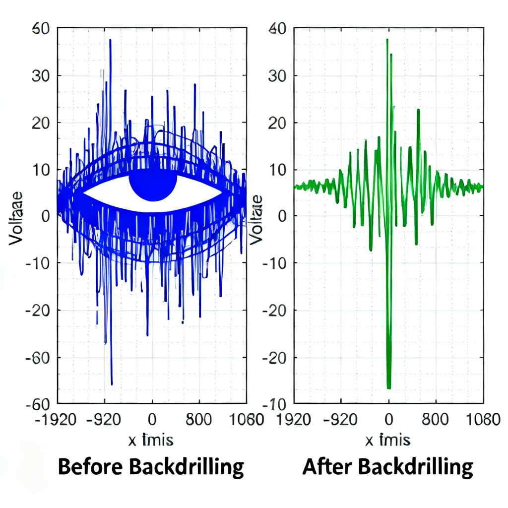
8. Simulation and Verification
Before manufacturing, simulate the effect of backdrilling. Use 3D EM simulation tools like Ansys HFSS, CST, or Keysight ADS to model the via with and without the stub, comparing S-parameters (S11, S21) and TDR impedance. Simulate the eye diagram with and without backdrilling; a closed eye at the target data rate indicates the need for backdrilling. After fabrication, use a time-domain reflectometer to measure the impedance profile of the via—a clean, flat impedance trace indicates successful backdrilling.
8.1 Example Simulation Results
Without backdrill, S21 shows a deep notch at 8 GHz (for a 120 mil stub in a 0.062″ board), and the eye diagram is completely closed at 10 Gbps. With backdrill, S21 is flat to 20 GHz, and the eye diagram is wide open with low jitter.
9. Conclusion: Backdrilling as a Design Necessity
Backdrilling is no longer a niche technique; it is a standard requirement for any PCB operating at high data rates. By removing the resonant via stub, it preserves signal integrity, reduces jitter, and ensures reliable operation of high-speed interfaces. If your signal operates above 1 Gbps, the cost of backdrilling is far less than the cost of a board spin due to SI failure. Specify clearly with exact depth, bit size, and tolerance in your fabrication notes. Partner with a capable manufacturer experienced in backdrilling, including X-ray inspection and depth control. Use 3D EM simulation to confirm the need and verify the improvement.
10. FAQ: Backdrilling PCB Questions
What is the recommended stub length after backdrilling?
For optimal signal integrity in backdrilling PCB applications, the target stub length should be less than 10 mils (0.25 mm) to minimize resonance effects in high-speed signals.
Can backdrilling be applied to all PCB layers?
Yes, backdrilling PCB can be applied to any layer, but it is most effective for signals on inner layers where the stub length is significant. It is commonly used for high-speed digital and RF designs.
How does backdrilling affect impedance control?
Backdrilling PCB removes the capacitive stub that causes impedance discontinuities, resulting in a more consistent impedance profile along the signal path, which is critical for maintaining signal integrity.
Is backdrilling necessary for differential pairs?
Yes, for high-speed differential pairs, backdrilling PCB is highly recommended to maintain symmetry and reduce common-mode noise caused by stub resonance, especially for interfaces like PCIe Gen 4/5 and 100G Ethernet.