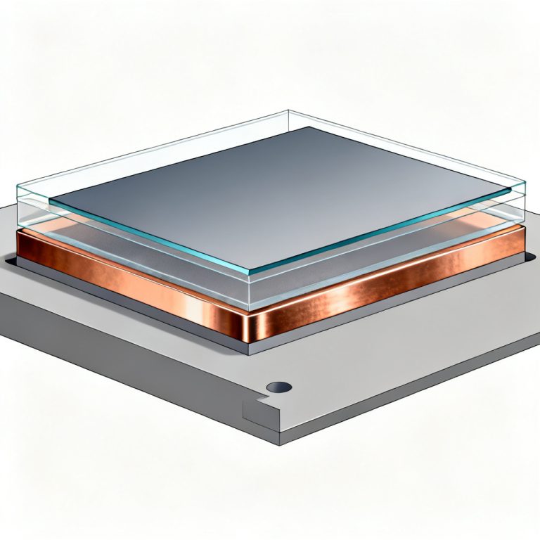
Microvia reliability is the cornerstone of High-Density Interconnect (HDI) PCB performance, directly determining product lifespan in aerospace, automotive, and medical devices. This definitive guide covers the three pillars of microvia reliability: copper plating chemistry, via stacking architecture, and thermal stress testing.
1. The Foundation – The Metallurgy of Microvia Plating
The reliability of a microvia is not determined by its diameter, but by the quality of the copper that lines its walls. A poorly plated microvia is a ticking time bomb.
1.1 The Void Problem (Inner Corner Separation)
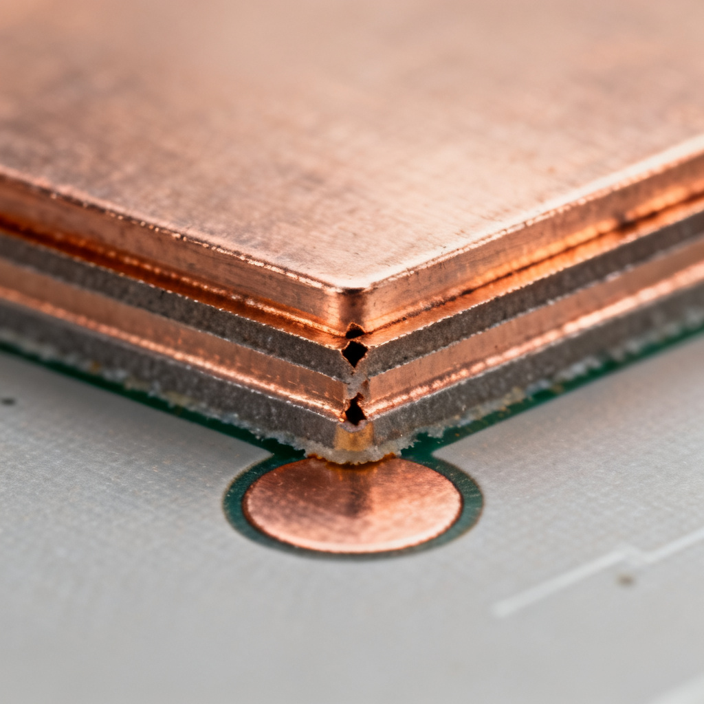
The most common failure mode in microvias is inner corner separation (also known as “corner cracking” or “voiding at the knee”). This occurs at the sharp transition point where the sidewall meets the target pad at the bottom of the via.
Why it happens:
- Insufficient Plating: If the copper deposit is too thin, it cannot withstand the stress of thermal cycling.
- Contamination: Resin smear or drilling debris left on the target pad prevents proper copper-to-copper adhesion.
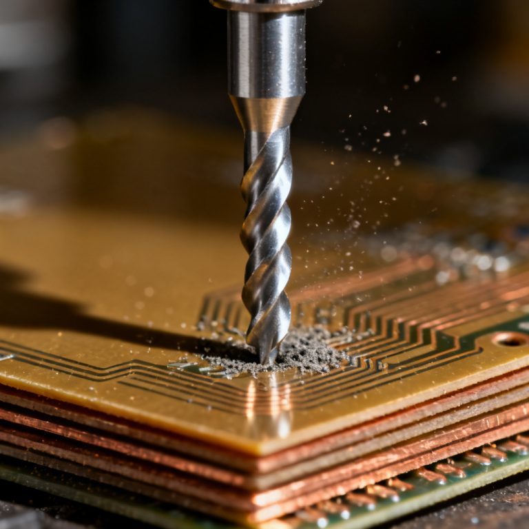
- Aspect Ratio Limits: As microvias get deeper (higher aspect ratio), the ability of plating solution to flow into the hole becomes limited, leading to a thinner deposit at the bottom.
1.2 Best Practices for Plating Chemistry and Process
To achieve a Class 3 / IPC-6012 high-reliability microvia, the plating process must be optimized:
- Electroless Copper (Seed Layer): This initial layer must be continuous and free of nodules. A poor electroless layer will result in “skip plating” where the subsequent electroplating fails to adhere.
- Electrolytic Copper (Fill): The copper must be “tensile” or “compressive” in nature, not “elongated.” Elongated grains are brittle and prone to cracking under thermal stress.
- Uniformity: The plating thickness at the bottom of the via should be at least 20 microns (0.8 mils) for standard reliability, and 25 microns (1.0 mils) for high-reliability applications. The ratio of thickness at the top of the via to the bottom should be close to 1:1.
- The Role of Levelers and Brighteners: Proprietary additives in the plating bath ensure that the copper deposits evenly inside the small hole, preventing “dog-boning” (excess copper at the top of the via) which can trap air and create voids.
1.3 The “Buried Via” Advantage
For the highest reliability, consider buried vias. Unlike blind vias that start on an outer layer and stop on an inner layer, buried vias are completely encased within the PCB. They are not subjected to the same level of mechanical stress during component assembly (soldering) and are statistically less likely to fail. However, they add cost and complexity to the lamination process.
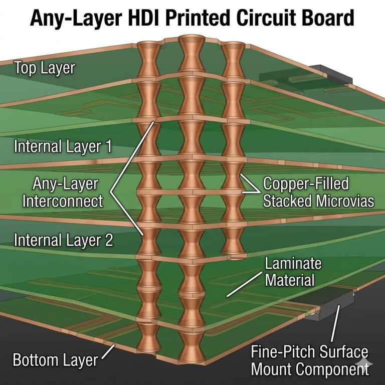
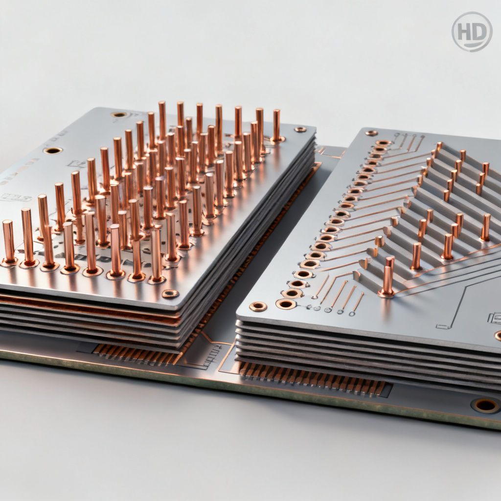
2. The Architecture – Stacking Microvias (Type I, II, III, IV)
You cannot simply stack microvias on top of each other like bricks. The geometry of the stack determines whether the structure will survive 1,000 thermal cycles or crack after 100.
2.1 The Geometry of Failure: Stacked vs. Staggered
- Staggered Microvias: This is the safest, most reliable structure. Vias on adjacent layers are offset from each other. This creates a “waffle” pattern of copper pads that distributes stress across a wider area. Recommendation: Use staggered vias whenever possible.
- Stacked Microvias: Vias are placed directly on top of each other, creating a vertical column of copper. This is space-efficient but highly stressed. The critical failure point is the interface between the top via and the bottom via.
2.2 The “Filled Via” Requirement for Stacked Structures
If you must use stacked microvias, the industry consensus is clear: The bottom via must be 100% filled with copper.
- Why? An unfilled stacked via creates a “tube within a tube.” When the PCB expands during heating, the inner tube pushes against the outer tube, creating massive stress at the interface. This leads to interface delamination.
- The Process: After drilling and plating the first via, it is filled with a specialized copper plating process (often using a low-current, high-additive chemistry). The surface is then planarized (flattened) before the next layer is laminated and drilled.
2.3 Stacking Architecture (Type I, II, III, IV)
Understanding the IPC classification helps you specify the correct structure:
- Type I (1 Build-up Layer): One layer of microvias on one side. Simplest, most reliable.
- Type II (2 Build-up Layers): Two layers of microvias on one side. Staggering is strongly recommended.
- Type III (2 Build-up Layers + Buried Via): Two microvia layers on top of a buried via core. The buried via can be a standard through-hole or a filled via.
- Type IV (3+ Build-up Layers): Three or more sequential microvia layers. This is where reliability becomes critical. Stacked vias of more than 2 layers are extremely risky without perfect filling and planarization.
2.4 The “Via-in-Pad” Problem
Placing a microvia directly on a BGA pad is a common practice for space savings, but it creates a solder void problem. During reflow, the air trapped inside the microvia (if unfilled) expands and pushes the solder away, creating a weak solder joint.
- The Solution: The microvia must be filled and capped. The via is filled with copper (or a non-conductive epoxy) and then a flat copper cap is plated over the top. This creates a solid, flat pad for the BGA ball.
3. The Proof – Thermal Stress Testing (The “Sixer” and Beyond)
No amount of theoretical design can replace physical testing. The industry standard for proving microvia reliability is thermal stress testing.
3.1 The IPC-TM-650 Test (The “Sixer”)
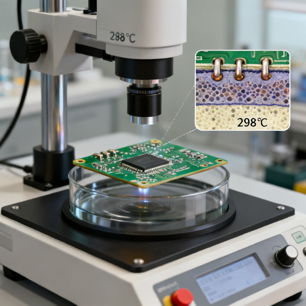
The most common test is IPC-TM-650 Method 2.6.27, often called the “Sixer” test.
- The Procedure: A coupon (test sample) is subjected to 6 cycles of solder float. Each cycle is: 10 seconds in 288°C (550°F) solder, followed by a cool-down to room temperature.
- The Pass/Fail Criteria: After the six cycles, the coupon is cross-sectioned and inspected under a microscope (50x to 200x magnification).
- Pass: No cracks, separations, or voids visible at the microvia inner corners, interface, or target pad.
- Fail: Any crack >50% of the copper thickness is a failure.
3.2 Beyond the Solder Float: Thermal Cycling (TCT)
While the “Sixer” tests for sudden thermal shock, Thermal Cycling (TCT) tests for fatigue over time. This is more relevant for automotive and aerospace applications.
- The Procedure: Samples are cycled between extreme temperatures (e.g., -55°C to +125°C) for 1,000 to 3,000 cycles. The ramp rate (how fast the temperature changes) is critical. Faster ramp rates induce more stress.
- Failure Mode: TCT reveals fatigue cracking. Unlike the sudden shock of solder float, TCT causes the copper to work-harden and crack over time. This is often seen as a “star crack” or “circumferential crack” at the via bottom.
3.3 Interpreting the Results: The “Pillar” of Confidence
What do the test results tell you?
- If the “Sixer” passes but TCT fails: Your plating is strong enough to survive assembly (solder shock) but not strong enough for long-term thermal cycling. This indicates a need for thicker copper or a different grain structure.
- If the “Sixer” fails: Your plating process is fundamentally flawed. You have voids, contamination, or insufficient thickness.
- The “Pillar” Test (Cross-Section Analysis): The most revealing test is a cross-sectional analysis of the microvia. Under high magnification, you can measure the exact copper thickness at the bottom, the sidewalls, and the top. You can also look for “pillar” or “column” growth of copper grains. A uniform, fine-grained copper structure is the “pillar” of reliability.
3.4 The Role of Laminate Material
The reliability of the microvia is also dependent on the CTE (Coefficient of Thermal Expansion) of the laminate material (e.g., FR-4, Polyimide, Rogers).
- The Problem: If the laminate expands much more than the copper (which is typical), the copper via is placed under tensile stress during heating.
- The Solution: Use a laminate with a low Z-axis CTE (e.g., <50 ppm/°C). High-Tg (Glass Transition Temperature) materials are essential for microvia reliability. Low-Tg materials will soften and expand excessively, tearing the microvia apart.
4. A Practical Checklist for Engineers
To ensure your next HDI design is reliable, use this checklist when reviewing your PCB manufacturer’s capabilities:
| Checklist Item | Microvia Reliability Specification | Acceptance Criteria |
|---|---|---|
| Plating Thickness | Minimum 20µm at bottom of microvia | Cross-section report required |
| Stacking Style | Default to staggered; use stacked only if necessary | 100% copper fill + planarization for stacked |
| Test Coupons | IPC-TM-650 Method 2.6.27 (Sixer) + Thermal Cycling (1000 cycles) | No cracks >50% copper thickness |
| Material Selection | High-Tg (170°C+) laminate with low Z-axis CTE | Low-Tg materials rejected |
| Aspect Ratio | Depth/diameter below 1:1 | 100µm deep via = 100µm diameter minimum |
| Surface Finish | ENIG or ENEPIG over filled and capped via | No solder voids in via-in-pad designs |
5. Conclusion: Reliability is a Process, Not a Checkbox
Microvia reliability is not achieved by a single design rule or a single test. It is a chain of excellence that starts with the plating chemistry, continues with the stacking architecture, and is proven by thermal stress testing.
By understanding the metallurgy of the copper, the geometry of the stack, and the brutality of the test, you can specify a PCB that will survive the harshest environments. When in doubt, default to staggered vias, demand 100% copper fill for stacked vias, and always ask for the cross-section report.
Frequently Asked Questions (FAQ)
What is microvia reliability and why is it important for HDI PCBs?
Microvia reliability refers to the ability of laser-drilled microvias to withstand thermal and mechanical stress without cracking or delaminating. It is critical for HDI PCBs used in aerospace, automotive, and medical devices where failure is not an option.
How do stacked microvias differ from staggered microvias in terms of reliability?
Staggered microvias are significantly more reliable than stacked microvias because they distribute stress across a wider area. Stacked microvias require 100% copper fill and planarization to avoid interface delamination under thermal cycling.
What thermal stress testing standards are used to validate microvia reliability?
The primary standard is IPC-TM-650 Method 2.6.27 (the “Sixer” test), which involves 6 cycles of solder float at 288°C. Thermal Cycling (TCT) between -55°C and +125°C for 1,000 to 3,000 cycles is also used for fatigue testing.
What is the “pillar” test in microvia reliability analysis?
The “pillar” test refers to cross-sectional analysis of microvias under high magnification to measure copper thickness at the bottom, sidewalls, and top. A uniform, fine-grained copper structure is considered the “pillar” of reliability.
How does laminate material affect microvia reliability?
The Coefficient of Thermal Expansion (CTE) of the laminate directly impacts microvia reliability. High-Tg materials with low Z-axis CTE prevent the laminate from expanding excessively and tearing the copper via apart during thermal cycling.
About the Author
This guide was compiled from the leading technical resources in the HDI PCB industry, including IPC standards, materials science papers, and the manufacturing best practices of top-tier PCB fabricators. For a detailed quote on your next high-reliability HDI project, contact our engineering team.