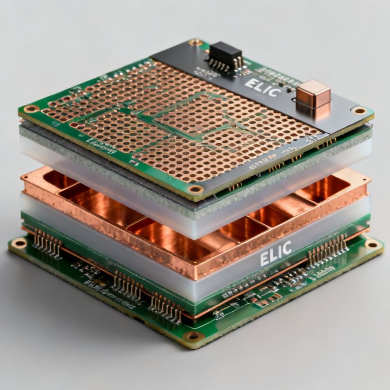
The mSAP process and fine line technology are the foundation of modern IC Substrates and SLP PCBs, enabling ultra-high-density interconnects for advanced electronics. This guide delivers a comprehensive, authoritative analysis of the modified Semi-Additive Process (mSAP), its role in achieving line/space (L/S) below 30µm, and the critical design rules for IC Substrates and Substrate-Like PCBs (SLP).
Understanding Core Technologies: IC Substrate & SLP PCB via mSAP Process
What is an IC Substrate?
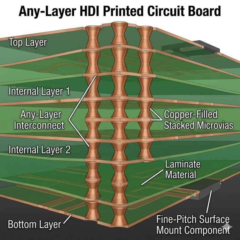
An IC Substrate is a specialized PCB that provides mechanical support, electrical interconnection, and thermal dissipation for a single integrated circuit die or multi-chip module. It bridges the ultra-fine pitch (40-80µm) of the die to a wider pitch (200-400µm) for the next level of interconnection. Applications include high-performance computing (CPU/GPU), memory modules, automotive ADAS, and RF modules. Key characteristics include extremely high layer count (up to 20+), ultra-fine L/S down to 8µm/8µm, and advanced materials like ABF and BT resin.
What is SLP (Substrate-Like PCB)?
SLP, often called mSAP HDI, is a high-density interconnect PCB that adopts IC substrate manufacturing techniques to achieve L/S below 30µm/30µm. It is a cost-effective alternative for high-end consumer electronics like smartphones, tablets, and wearables. Unlike standard HDI (limited to 50µm/50µm via subtractive etching), SLP uses the mSAP process to achieve L/S of 20µm/20µm or finer.
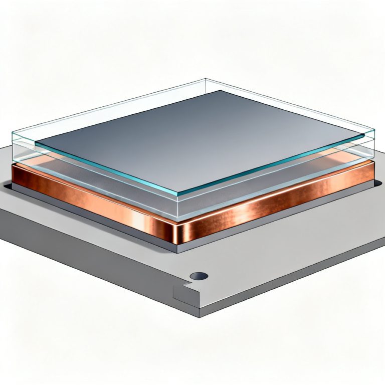
The mSAP Process: The Manufacturing Revolution
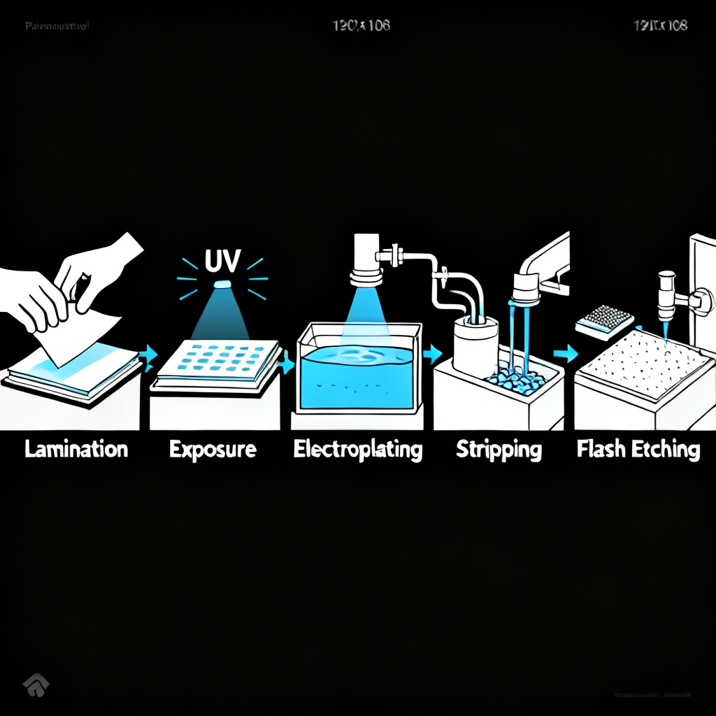
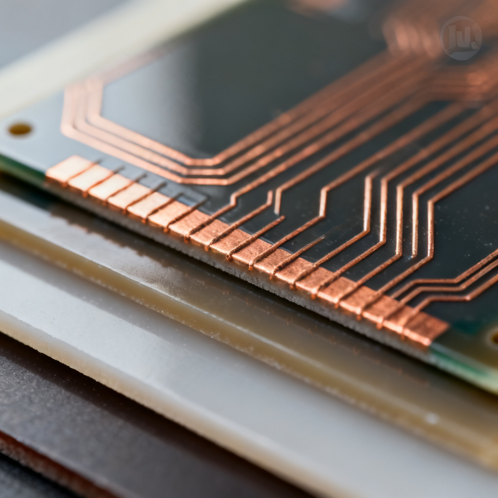
The modified Semi-Additive Process (mSAP) is the cornerstone technology enabling fine line features. Unlike traditional subtractive processes, mSAP builds up copper only where needed. The process flow includes: lamination of a thin seedless copper foil (1-3µm), dry film lamination and exposure, copper electroplating into photoresist openings, photoresist stripping, flash etching to remove the seed layer, and surface treatment. mSAP achieves superior fine line resolution (down to 8µm/8µm), improved uniformity with near-vertical sidewalls, and reduced undercut.
Fine Line Technology: Design Rules & Capabilities for mSAP Process
What is “Fine Line” in PCB Context?
In the industry, “fine line” refers to conductor widths and spacing below 50µm. For IC Substrates, it is sub-30µm; for SLP, it is typically 20-30µm. The following table summarizes technology levels:
| Technology Level | Line/Space (L/S) | Typical Application | Process |
|---|---|---|---|
| Standard HDI | 75µm/75µm (3/3 mil) | Consumer electronics | Subtractive |
| Advanced HDI | 50µm/50µm (2/2 mil) | Automotive, IoT | Subtractive |
| SLP (mSAP) | 20µm/20µm (0.8/0.8 mil) | Smartphones, Wearables | mSAP |
| IC Substrate | 8µm/8µm (0.3/0.3 mil) | CPU/GPU, Memory | mSAP / SAP |
Critical Design Considerations for Fine Lines
When designing for mSAP processes, engineers must account for impedance control (tight tolerance for 50Ω or 100Ω differential), aspect ratio (AR) of trace height to width (typically 1:1 to 1.5:1), copper roughness (smoother surface reduces signal loss at high frequencies), and via-in-pad (VIP) registration.
Material Selection for mSAP
The choice of dielectric material is paramount for fine-line performance. ABF (Ajinomoto Build-up Film) is the gold standard for IC Substrates, offering low CTE, high Tg, and excellent adhesion. BT (Bismaleimide Triazine) is common for memory modules. Modified epoxy is used for lower-cost SLP applications. LCP (Liquid Crystal Polymer) is used for high-frequency, flexible substrates.
IC Substrate vs. SLP: A Detailed Comparison
While both use mSAP, they serve different markets. The following table highlights key differences:
| Feature | IC Substrate | SLP (Substrate-Like PCB) |
|---|---|---|
| Primary Application | Single IC packaging (CPU, GPU, Memory) | Main logic board for mobile devices |
| Typical Line/Space | 8µm/8µm to 15µm/15µm | 20µm/20µm to 30µm/30µm |
| Layer Count | 6 to 20+ | 4 to 12 |
| Core Technology | mSAP, SAP | mSAP, modified SAP |
| Dielectric Material | ABF, BT (High-end) | Modified Epoxy, Low-loss materials |
| Via Type | Microvias (laser), Through-hole | Microvias (laser), Buried/blind vias |
| Cost per Layer | Very High | Moderate |
| Yield Sensitivity | Extremely high (defect = scrap die) | High (defect = scrap board) |
| Market Driver | Moore’s Law scaling, HPC | Miniaturization, thinner devices |
The line is blurring. High-end SLP designs now approach the complexity of entry-level IC Substrates. For example, some flagship smartphones use an SLP board with L/S of 18µm/18µm.
Manufacturing Challenges & Solutions in mSAP Process
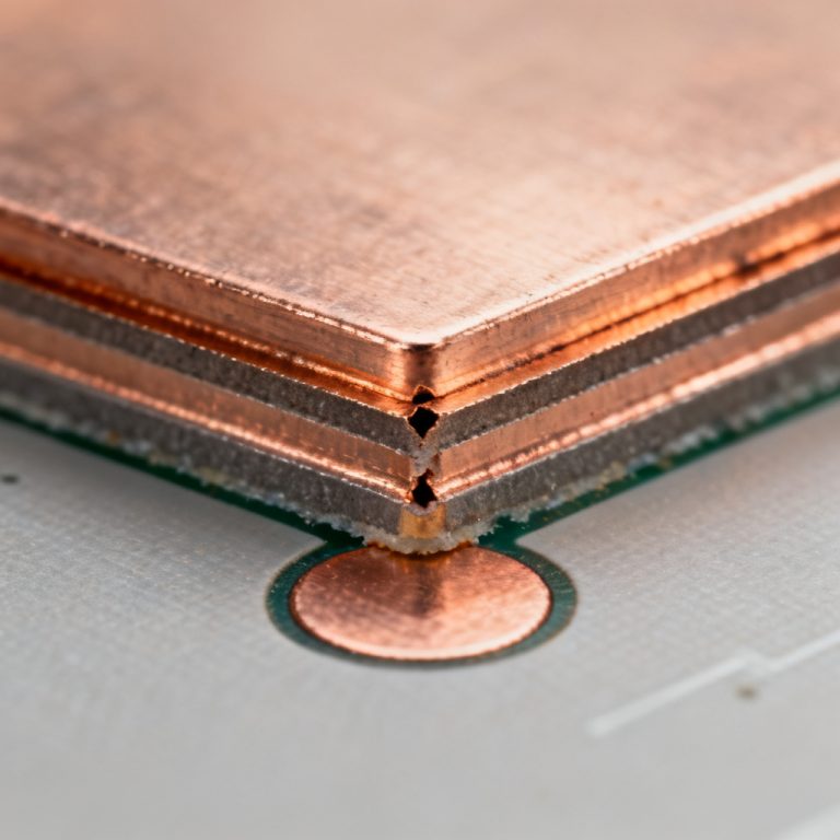
The Flash Etching Dilemma
The most critical process step in mSAP is flash etching. The goal is to remove the 1-3µm seed layer without etching the 15-20µm tall traces. If the etch is too aggressive, trace sidewalls are undercut. Solution: Advanced wet etching chemistry with high selectivity, combined with real-time endpoint detection systems.
Registration & Alignment
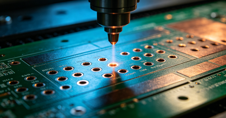
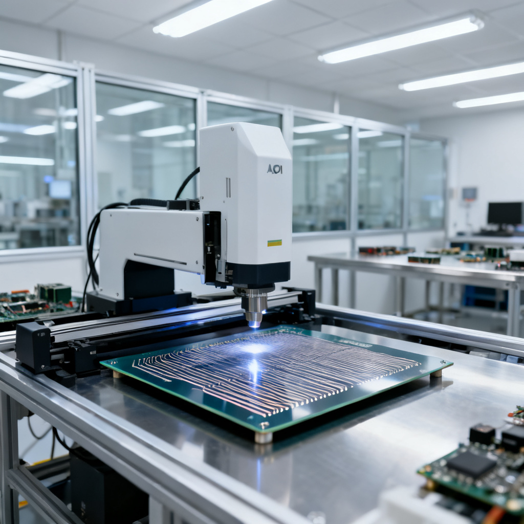
With features as small as 8µm, alignment between layers is a major yield killer. Solution: High-precision laser direct imaging (LDI) systems with automated optical alignment (AOI) feedback loops, ensuring via-to-pad registration within ±5µm.
Plating Uniformity
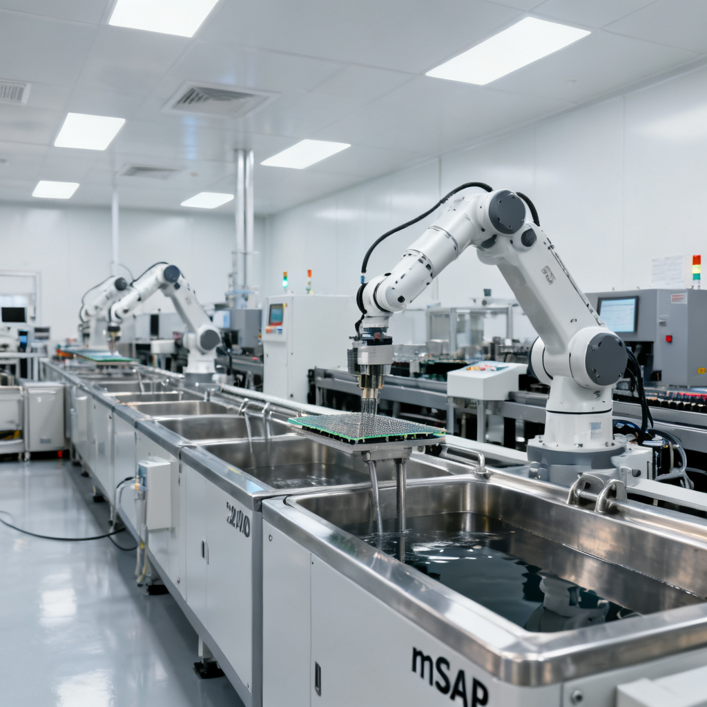
Electroplating copper into fine trenches requires high throwing power and careful current density management. Solution: Use of pulse plating (reverse pulse) to improve deposit uniformity, combined with advanced paddle agitation systems.
Defect Inspection
Detecting defects on boards with 8µm lines requires more than traditional AOI. Solution: High-resolution AOI (1µm pixel size), automated X-ray inspection (AXI), and electrical test with fine probe tips.
The Future of mSAP & Fine Line Technology
The Push to Sub-5µm
The next frontier is achieving L/S of 5µm/5µm and below, requiring a move from mSAP to SAP (Semi-Additive Process), where no seed layer is used. This eliminates the flash etching step entirely.
Hybrid Bonding & 3D Packaging
For advanced IC Substrates, fine line technology is combined with hybrid bonding (Cu-Cu direct bonding) to achieve interconnects with pitches less than 1µm.
Material Innovation
New dielectrics with lower Dk and Df are being developed for 112Gbps and 224Gbps SerDes data rates. Materials like PTFE-based composites and advanced liquid crystal polymers are tailored for mSAP compatibility.
Cost Reduction for Mainstream Adoption
The holy grail is reducing mSAP cost for mid-range consumer electronics and automotive applications. This involves panel size scaling, process automation, and dry film innovation.
Why mSAP Matters for Your Next Project
Whether designing the next flagship smartphone or a high-performance computing module, understanding the mSAP process and fine line technology is a competitive necessity. IC Substrates and SLP PCBs enable modern electronics, and mastering their manufacturing nuances is key to achieving density, performance, and reliability.
At [Your Company Name], we specialize in high-precision mSAP manufacturing. Our facilities handle L/S down to 8µm/8µm for IC Substrates and 20µm/20µm for SLP boards. We combine advanced process control with rigorous quality assurance. Contact our engineering team for a free DFM review and custom quote.
FAQ: IC Substrate & SLP PCB with mSAP Process
What is the mSAP process used for in PCB manufacturing?
The mSAP process is used to create ultra-fine line features (down to 8µm/8µm) for IC Substrates and SLP PCBs, enabling high-density interconnects in advanced electronics like smartphones, CPUs, and memory modules.
How does SLP differ from standard HDI?
SLP (Substrate-Like PCB) uses the mSAP process to achieve L/S of 20µm/20µm or finer, while standard HDI is limited to 50µm/50µm due to subtractive etching.
What materials are best for the mSAP process?
ABF and BT are preferred for IC Substrates, while modified epoxy is used for SLP. Material selection depends on the required fine line technology performance and cost targets.
What are the main challenges in mSAP manufacturing?
Key challenges include flash etching control, registration alignment, plating uniformity, and defect inspection. Solutions involve advanced chemistry, LDI systems, pulse plating, and high-resolution AOI.