In the realm of modern electronics, RF & microwave PCB design operates at frequencies from 300 MHz to 300 GHz, requiring meticulous material selection and fabrication to manage signal integrity, impedance control, and EMI. This guide synthesizes expert knowledge from leading industry resources to provide a comprehensive overview of materials, design principles, and fabrication techniques for high-performance applications.
Whether you are designing for 5G communications, radar systems, or satellite links, understanding these fundamentals is critical to achieving reliable results.
Meta Description: Master RF & microwave PCB design with our guide on materials, fabrication, and impedance control. Learn from experts to achieve high performance for 5G, radar, and satellite applications.
Key Design Principles for RF & Microwave PCB Design
Impedance Control: The Cornerstone of RF & Microwave PCB Design
RF & microwave PCB design requires non-negotiable impedance matching. Any mismatch between the transmission line and the load (e.g., antenna, amplifier) causes signal reflections, power loss, and standing waves. For RF circuits, controlled impedance (typically 50Ω, 75Ω, or 100Ω differential) must be maintained across the entire signal path. Key factors influencing impedance include:
- Trace width and thickness: Wider traces lower impedance; thinner traces increase it.
- Dielectric constant (Dk) of the substrate: A higher Dk reduces impedance for a given trace width.
- Substrate thickness: Thicker substrates increase impedance for microstrip lines.
- Copper foil roughness: Rougher copper increases conductor losses at high frequencies.
Designers must use impedance calculators (e.g., from IPC-2141A or tools like Polar Si9000) and specify tolerance (typically ±10% for RF, tighter for microwave).
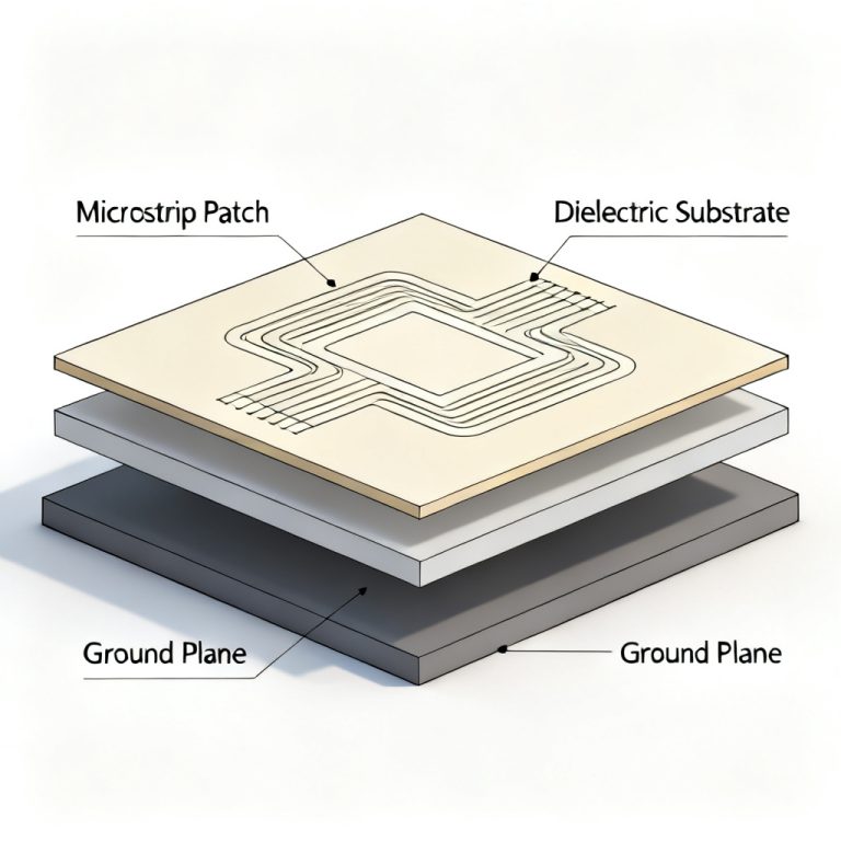
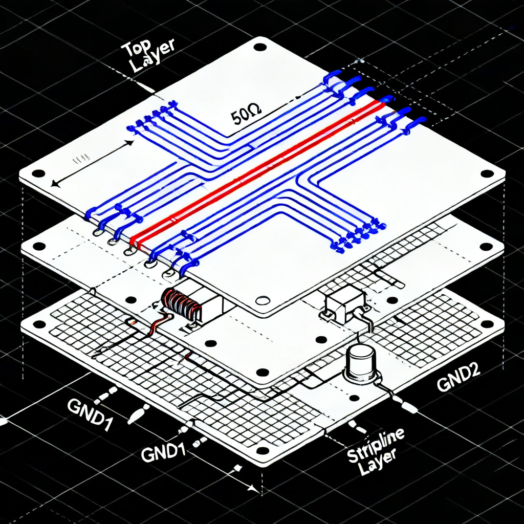
Transmission Line Topologies: Microstrip vs. Stripline
Two primary transmission line structures are used in RF & microwave PCB design:
- Microstrip: A trace on the outer layer with a ground plane below. It’s easier to fabricate and modify but more susceptible to radiation and EMI. Suitable for frequencies up to ~20 GHz.
- Stripline: A trace sandwiched between two ground planes. It offers better isolation and lower radiation but requires more layers and precise alignment. Preferred for frequencies above 10 GHz and for critical signals.
For high-density designs, coplanar waveguide (CPW) with ground is another option, balancing ease of routing with good shielding.
Signal Integrity & Loss Management in RF & Microwave PCB Design
At RF frequencies, signal degradation comes from:
- Dielectric loss (tan δ): Caused by the substrate’s dissipation factor. Low-loss materials (e.g., PTFE, Rogers) are essential.
- Conductor loss: Skin effect concentrates current at the surface of copper traces. Use smooth copper (e.g., rolled annealed) and wider traces where possible.
- Radiation loss: From open structures like microstrip; minimize by using stripline or adding shielding vias.
To maintain signal integrity:
- Keep trace lengths short and direct.
- Avoid 90-degree corners; use 45-degree chamfers or curved bends.
- Use ground vias near signal vias to reduce parasitic inductance.
Grounding and Shielding Techniques for RF & Microwave PCB Design
Proper grounding is critical to reduce noise and EMI:
- Solid ground planes: Avoid split planes under RF traces. Use a continuous ground reference.
- Via stitching: Place ground vias around the perimeter of RF areas and along transmission lines to create a Faraday cage effect.
- Shielding cans: For sensitive components (e.g., VCOs, PLLs), use metal shields soldered to the ground plane.
Component Placement and Routing
- Place RF components (e.g., amplifiers, filters) close together to minimize trace length.
- Keep power supply traces away from RF paths.
- Use decoupling capacitors (low ESL/ESR types) near active devices.
- For differential pairs (e.g., in 5G or high-speed digital), ensure equal length and tight coupling.
Materials for RF & Microwave PCB Design
Critical Material Properties for RF & Microwave PCB Design
Selecting the right substrate is the most impactful decision in RF & microwave PCB design. Key parameters:
- Dielectric Constant (Dk): Should be stable across frequency and temperature. Variation causes impedance drift.
- Dissipation Factor (Df or tan δ): Lower values (e.g., <0.002) reduce signal loss.
- Thermal Conductivity: Higher values (e.g., >0.5 W/m·K) aid heat dissipation from high-power RF components.
- Coefficient of Thermal Expansion (CTE): Match with copper to prevent delamination during soldering or thermal cycling.
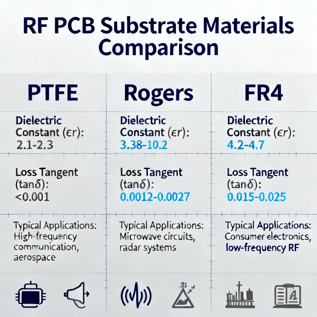
Common RF Substrate Materials for RF & Microwave PCB Design
| Material Type | Examples | Dk (at 10 GHz) | Df (at 10 GHz) | Typical Applications |
|---|---|---|---|---|
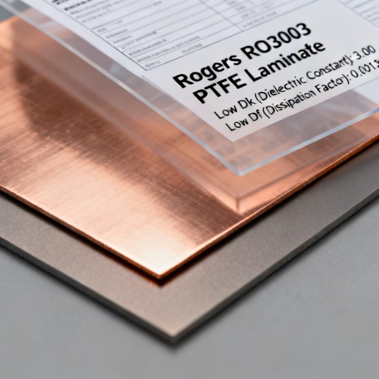
| PTFE (Teflon) | Rogers 3000/4000 series, Taconic RF-35 | 2.2 – 3.5 | 0.0009 – 0.0025 | High-frequency, low-loss; 5G, radar, satellite |
| Hydrocarbon/Ceramic | Rogers RO4000 series, Isola Astra MT77 | 3.0 – 3.7 | 0.002 – 0.003 | Mid-range RF; automotive radar, base stations |
| FR-4 (High-performance) | Isola 370HR, ITEQ IT-180A | 4.2 – 4.5 | 0.015 – 0.020 | Low-cost, low-frequency RF (<1 GHz) |
| Polyimide | Kapton, DuPont | 3.4 – 3.5 | 0.005 – 0.010 | Flexible circuits, high-temperature environments |
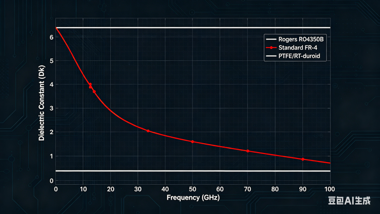
Note: FR-4 is generally unsuitable above 1 GHz due to high loss and Dk variation. For microwave frequencies (>5 GHz), PTFE-based laminates are preferred.
Copper Foil Selection for RF & Microwave PCB Design
- Standard electrodeposited (ED) copper: High roughness (typically 2-5 μm Ra), leading to higher conductor loss. Suitable for low-frequency RF.
- Rolled annealed (RA) copper: Smoother (0.3-0.5 μm Ra), reduces skin effect losses. Essential for microwave designs.
- Reverse treated foil (RTF): A compromise between ED and RA, offering moderate smoothness and good adhesion.
Prepreg and Bonding Materials
For multilayer RF PCBs, prepregs must match the core material’s Dk and Df. Use low-loss prepregs (e.g., Rogers 4450F or Isola 408HR) to maintain consistent impedance across layers.
Fabrication Process for RF & Microwave PCB Design
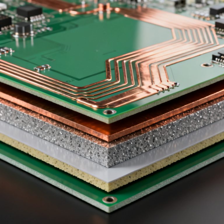
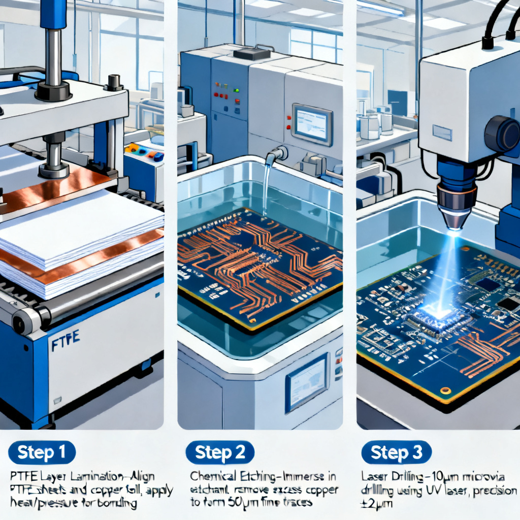
Lamination and Layer Stack-up
- Symmetrical stack-up: Avoid warpage by balancing copper thickness and layer count.
- Controlled dielectric thickness: Use thin, uniform prepreg layers (e.g., 0.004” to 0.008”) for tight impedance control.
- High-temperature lamination: PTFE materials require higher pressure and temperature (e.g., 350°C) than standard FR-4.
Etching and Tolerances
- Fine line etching: RF traces often require 3-5 mil widths. Use advanced etching techniques (e.g., plasma etching) to minimize undercut.
- Impedance tolerance: Fabricators must achieve ±10% or better. Use coupon testing on production panels to verify.
Via and Hole Technology
- Microvias: For high-density RF designs, laser-drilled microvias (diameter <0.006”) reduce parasitic inductance.
- Backdrilling: Remove unused stub portions of through-hole vias to eliminate resonance at high frequencies.
- Via filling: Use conductive or non-conductive fill to prevent solder wicking and maintain flat surfaces.
Surface Finishes
- ENIG (Electroless Nickel Immersion Gold): Excellent for RF due to flat surface and good solderability. Avoid for gold wire bonding (use ENEPIG instead).
- Immersion Silver: Lower cost, good for RF but prone to tarnishing.
- HASL (Hot Air Solder Leveling): Not recommended for RF due to uneven surface and lead content.
Testing and Quality Assurance
- TDR (Time Domain Reflectometry): Measure impedance of production boards.
- Network analyzer: Check S-parameters (e.g., S11, S21) for insertion loss and return loss.
- Thermal cycling: Verify reliability of material interfaces (e.g., CTE mismatch).
Advanced Considerations for High-Performance RF & Microwave PCB Design
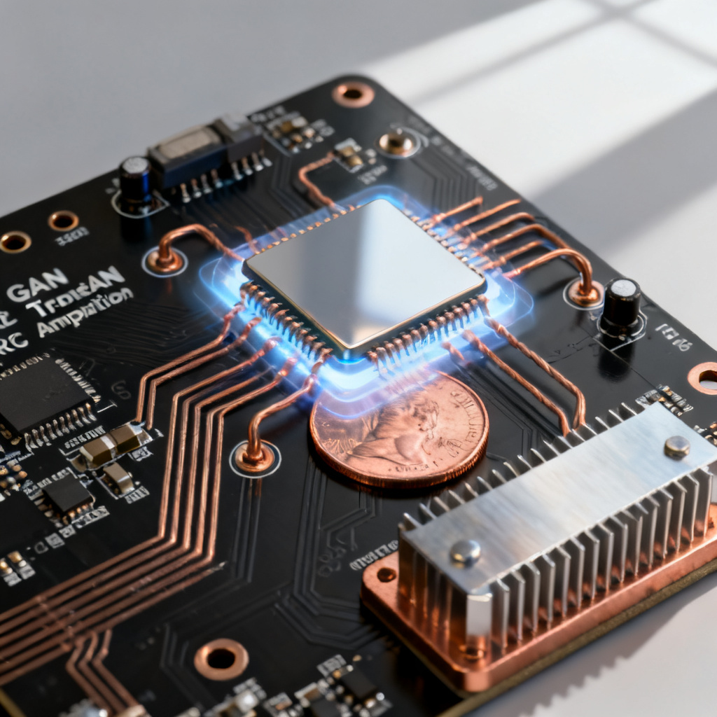
Thermal Management
High-power RF components (e.g., GaN amplifiers) generate significant heat. Solutions include:
- Thermal vias: Array of vias under heat-generating components, connected to a copper coin or heat sink.
- Metal-core PCB: Use aluminum or copper base for direct heat dissipation.
- Embedded copper blocks: For extreme power levels, embed copper blocks in the PCB.
Electromagnetic Compatibility (EMC)
- Filtering: Add ferrite beads or low-pass filters on power lines.
- Shielding: Use conductive gaskets or EMI gaskets around enclosure seams.
- Grounding: Ensure low-impedance ground return paths for all RF currents.
Design for Manufacturability (DFM)
- Minimum trace/space: Check with your fabricator (e.g., 4/4 mil for RF, tighter for advanced processes).
- Aspect ratio for vias: Keep via diameter to board thickness ratio < 10:1 to ensure plating reliability.
- Panel utilization: Optimize board size to reduce waste and cost.
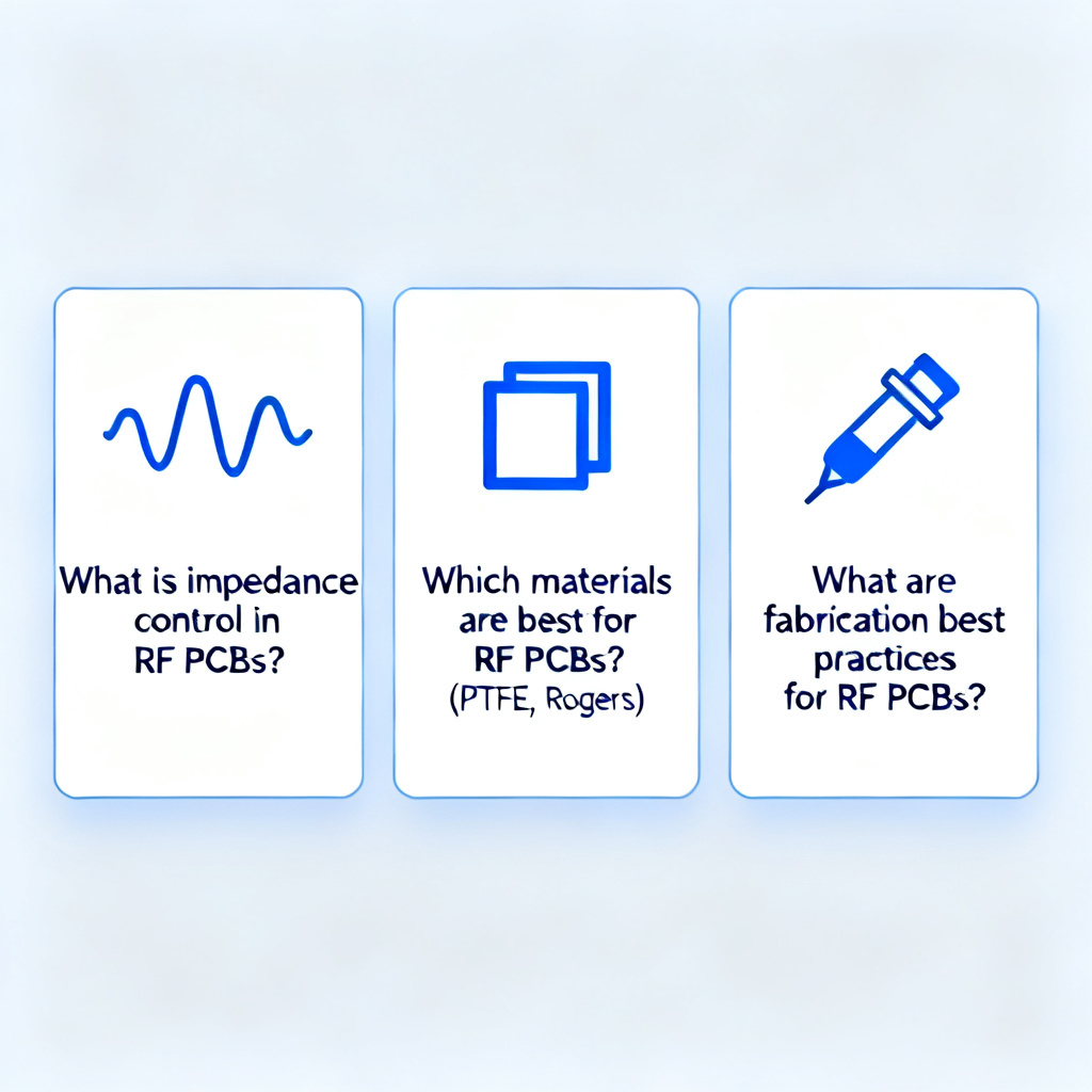
Frequently Asked Questions (FAQ) about RF & Microwave PCB Design
What is the most important material property for RF & microwave PCB design?
The most important property is the dissipation factor (Df) because it directly impacts signal loss. Low Df materials like PTFE are essential for high-frequency performance.
Why is impedance control critical in RF & microwave PCB design?
Impedance control prevents signal reflections and power loss, ensuring that the RF signal travels efficiently from the source to the load. Without it, performance degrades significantly.
Can FR-4 be used for RF & microwave PCB design?
FR-4 is generally unsuitable above 1 GHz due to high loss and unstable dielectric constant. For frequencies above 1 GHz, PTFE or hydrocarbon/ceramic materials are recommended.
What surface finish is best for RF & microwave PCB design?
ENIG (Electroless Nickel Immersion Gold) is widely preferred for RF due to its flat surface and excellent solderability, which helps maintain consistent impedance.
How does copper foil roughness affect RF & microwave PCB design?
Rougher copper increases conductor loss due to the skin effect. Rolled annealed (RA) copper with smooth surface is ideal for microwave frequencies to minimize losses.
Our Service: High-Performance RF & Microwave PCB Fabrication
We specialize in RF & microwave PCB design and fabrication, offering advanced materials (PTFE, Rogers, Taconic), controlled impedance, backdrilling, and TDR testing. Our DFM support ensures your design is manufacturable and cost-effective. Contact us for a quote or consultation on your next high-frequency project.