In the realm of high-speed digital PCBs, maintaining pristine Signal Integrity is the defining challenge of modern electronics design. As data rates push from 25G NRZ into the 224G PAM4 frontier, the physical interconnect—the PCB itself—becomes the primary bottleneck in SerDes channel performance. This comprehensive High-Speed Digital PCBs resource provides a physics-to-manufacturing blueprint for engineers navigating the complexities of Signal Integrity & SerDes implementation in advanced computing and AI infrastructure.
Foundational Concepts: Signal Integrity and the SerDes Architecture
High-speed digital PCBs rely on a Serializer/Deserializer (SerDes) to convert parallel data into a high-speed serial stream. Signal Integrity in these high-speed digital PCBs is limited not by the silicon alone, but by the Channel Loss Budget.
Defining the Signal Integrity Framework for High-Speed Digital PCBs
Before detailed layout begins, engineers working on high-speed digital PCBs must establish a clear cognitive framework for SerDes challenges. These challenges categorize into three primary degradation mechanisms:
- Impedance Discontinuities: Reflections caused by sudden changes in the transmission line geometry.
- Attenuation (Insertion Loss): The weakening of the signal as it travels through the dielectric and copper medium.
- Crosstalk and Noise: Interference from adjacent signals or the power supply network.
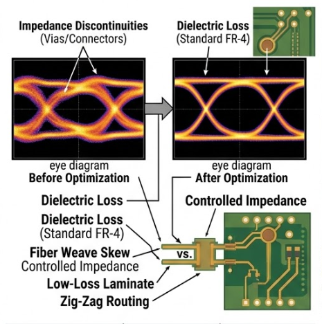
Important Priority Note for High-Speed Digital PCBs: While many designers obsess over routing corners (90-degree vs. 45-degree bends), corners and bends can generally be ignored at SerDes wavelengths in high-speed digital PCBs. The real enemy of Signal Integrity is the Via Stub and the Connector Interface.
The S-Parameter Mandate for SerDes Validation
To validate a SerDes channel on high-speed digital PCBs, the industry relies on Scattering Parameters (S-Parameters).
- S11 (Return Loss): A measure of how much signal energy is reflected back to the transmitter. High-speed SerDes channels require strict S11 limits to prevent the reflected wave from interfering with the transmitted symbol.
- S21 (Insertion Loss): The measure of signal amplitude reduction from Port 1 to Port 2. This is the most critical metric for PCB layout engineers working on high-speed digital PCBs.
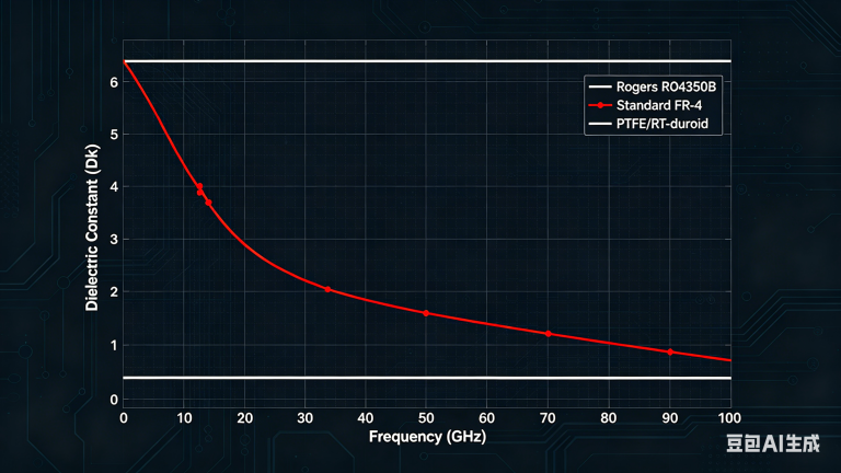
The Critical Role of Material Selection for High-Speed Digital PCBs
High-speed digital PCBs demand precise laminate selection. The choice of laminate is the single most impactful decision governing insertion loss (S21). At frequencies above 5 GHz, the dominant loss mechanism is Dielectric Loss.
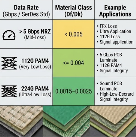
Dissipation Factor (Df) Thresholds in High-Speed Digital PCBs
The table below outlines the strict material thresholds required for high-speed digital PCBs to maintain acceptable Signal Integrity:
| Data Rate / SerDes Standard | Required Laminate Df Value | High-Speed Digital PCBs Material Classification |
|---|---|---|
| > 5 Gbps (NRZ) | Df < 0.005 | Mid-Loss |
| 112G PAM4 | Df ≤ 0.004 | Very Low Loss |
| 224G PAM4 | Df 0.0015–0.0025 | Ultra-Low Loss |
- For speeds > 5 Gbps: You must select laminates with a Dissipation Factor (Df) < 0.005. Standard FR-4 (Df ~0.020) will render a 10-inch 25Gbps link completely unusable on high-speed digital PCBs.
- For 112G PAM4 (56 Gbaud): Use Very Low Loss laminates (Df ≤ 0.004) on high-speed digital PCBs.
- For 224G PAM4 (112 Gbaud): Ultra-Low Loss laminates are mandatory for high-speed digital PCBs. Materials with Df values in the 0.0015–0.0025 range are required to meet the reach requirements of OSFP/QSFP-DD connectors.
Dielectric Constant (Dk) and Thermal Stability
- Stability: Look for materials with a Dk tolerance of +/- 0.05 across the operating frequency band to ensure consistent impedance on high-speed digital PCBs.
- Glass Transition Temperature (Tg): For high-speed digital PCBs destined for AI server racks with multiple reflow cycles and high operating ambient temperatures, Tg > 170°C is recommended. This prevents pad cratering and barrel fatigue during assembly.
Copper Foil Profile
Insertion loss on high-speed digital PCBs is also a function of conductor loss. The skin effect forces high-frequency current to the surface of the copper trace. Rough copper (Reverse Treat Foil) creates a longer electrical path than the physical length.
- Recommendation for High-Speed Digital PCBs: Use Low Profile (LP) or Very Low Profile (VLP) copper foil for all outer layer SerDes routing. The reduction in surface roughness significantly lowers insertion loss per inch on high-speed digital PCBs.
Transmission Line Theory and Impedance Control in SerDes Links
Every trace on high-speed digital PCBs is a transmission line. The goal is to maintain a consistent characteristic impedance (Z₀) from the silicon bump through the package, across the high-speed digital PCBs, and into the connector for optimal Signal Integrity.
Target Impedance for High-Speed Digital PCBs
- Single-Ended: 50Ω ±10% (Typically used for older clock lines or specific control signals on high-speed digital PCBs).
- Differential: 100Ω ±5% is the industry standard for high-speed SerDes pairs on high-speed digital PCBs. Tighter tolerance (e.g., ±5% vs. ±10%) is strongly recommended by chipset vendors to minimize reflection noise.
The Impact of Substrate Properties on High-Speed Digital PCBs
The impedance equation for high-speed digital PCBs is governed by trace width (W), spacing (S), height to reference plane (H), and the material’s Dk. Variations in the glass weave distribution (Resin Rich vs. Glass Rich areas) create localized Dk variations. This is particularly detrimental to PAM4 SerDes signals on high-speed digital PCBs, as discussed in Section 7.
Stackup Design Strategies for High-Speed Digital PCBs
A poor stackup on high-speed digital PCBs cannot be fixed with good routing.
Layer Count and Routing Strategy for SerDes
For systems with 100G+ SerDes interfaces, high-speed digital PCBs typically require 14 to 24 layers. The stackup must provide:
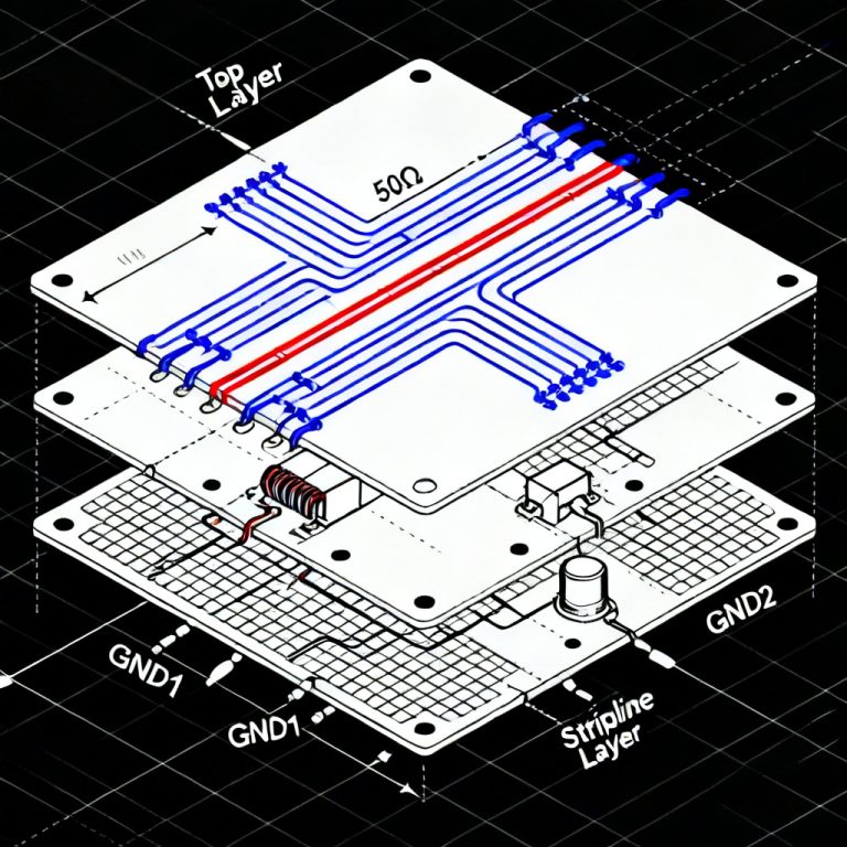
- Stripline Configuration: High-speed SerDes routing on high-speed digital PCBs must be placed on inner layers sandwiched between two solid reference planes. This ensures complete shielding and predictable impedance.
- Adjacent Ground: Never route high-speed SerDes signals adjacent to a split power plane on high-speed digital PCBs. The return current will find the path of least inductance, creating an unintentional loop antenna and massive EMI.
HDI (High-Density Interconnect) Requirements for High-Speed Digital PCBs
For large BGA packages (e.g., Network Switch ASICs with 1.0mm pitch or smaller) on high-speed digital PCBs:
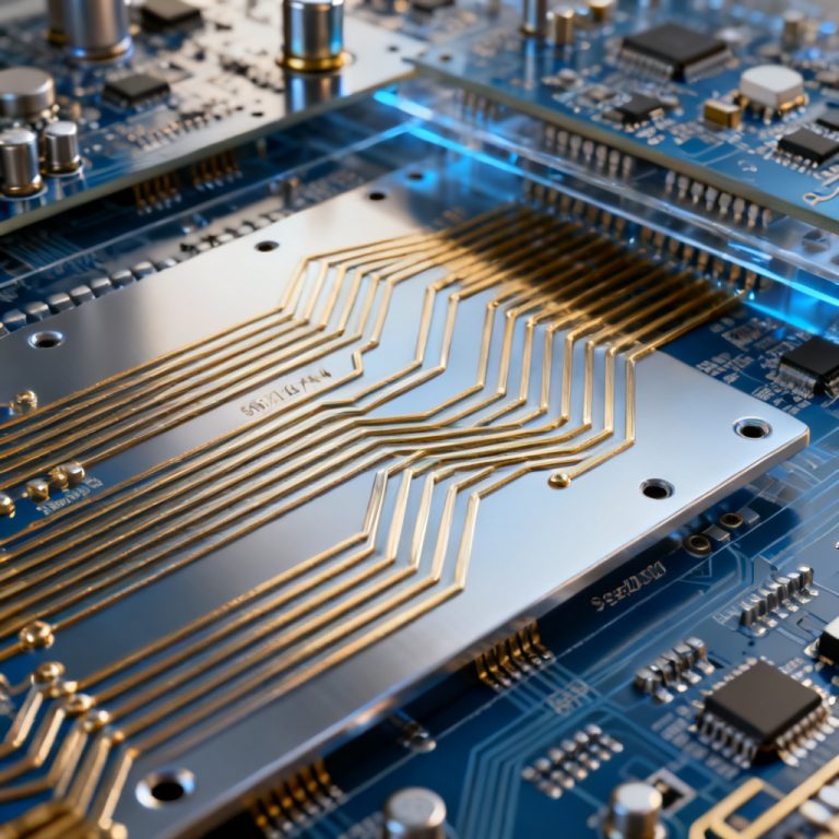
- Microvias: When BGA pitch reaches 0.8mm or smaller on high-speed digital PCBs, traditional through-hole vias become impossible to route between balls. Laser-drilled microvias (stacked or staggered) are required to fan out SerDes signals from the inner rows of the package while maintaining Signal Integrity.
Routing Topologies: Differential Pairs and Length Matching
Differential Pair Coupling on High-Speed Digital PCBs
- Tight Coupling vs. Loose Coupling: While tight coupling offers common-mode noise rejection on high-speed digital PCBs, loose coupling (larger spacing) is often preferred for ultra-high speed SerDes because it minimizes the sensitivity to glass weave skew (see Section 7.2).
- Spacing Rule for High-Speed Digital PCBs: Maintain at least 3W to 5W spacing to other traces (where W is the trace width) on high-speed digital PCBs to prevent Far-End Crosstalk (FEXT).
Length Matching (Phase Tolerance) in SerDes Design
Intra-pair skew destroys the differential SerDes signal eye on high-speed digital PCBs.
- P/N Matching: The length mismatch within a single differential pair on high-speed digital PCBs should be managed to within 1 to 5 mils (0.025mm to 0.127mm). For 112G PAM4 SerDes, tolerance should be tightened to the low end of this range.
- Lane-to-Lane Matching: For parallel SerDes interfaces like PCIe or XAUI on high-speed digital PCBs, skew between lanes must be managed according to the SerDes elastic buffer size, typically within 20-40 mils.
The Primary Discontinuity Culprits: Vias and Connectors
Via Optimization for High-Speed Digital PCBs (Anti-Pad and Backdrilling)
Vias represent a massive shunt capacitance on high-speed digital PCBs. The resonance of an unused via stub (the portion below the signal layer connection) can create a notch filter that eliminates the SerDes signal energy at exactly the Nyquist frequency.
- Backdrilling: For any via transitioning from top/bottom to an inner layer on high-speed digital PCBs, backdrilling is non-negotiable. The stub length must be kept under 10-15 mils to push the stub resonance well beyond the operating bandwidth of the SerDes link.
- Anti-Pad Sizing: Enlarging the clearance hole (anti-pad) around the via barrel on the reference planes of high-speed digital PCBs reduces parasitic capacitance. The design should balance anti-pad size with the plane’s current return path continuity.
Connector Launch Design on High-Speed Digital PCBs
The transition from PCB trace to the press-fit or SMT connector footprint is the weakest link in the SerDes channel on high-speed digital PCBs.
- SMT Pad Optimization: The size of the SMT pad on high-speed digital PCBs should be matched to the trace width. Large, unnecessary pad area creates a capacitive “bump” that degrades return loss (S11).
- Ground Stitching: Surround the high-speed SerDes connector pins on high-speed digital PCBs with a tight ring of ground vias to provide a low-inductance return path for the electric field.
Advanced Physical Effects: Copper Roughness and Fiber Weave
Copper Roughness Induced Loss in High-Speed Digital PCBs
As noted in Section 3.3, surface roughness increases the effective path length for current on high-speed digital PCBs. This is modeled using the Hammerstad Roughness Correction Factor. For 224G PAM4 SerDes, the difference between Standard Electro-Deposited (ED) copper and HVLP (Hyper Very Low Profile) copper can be 1-2 dB per inch on high-speed digital PCBs.
The Fiber Weave Effect (Skew) on Signal Integrity
FR4 and similar laminates used in high-speed digital PCBs are composites of woven glass fiber and epoxy resin. Glass has a lower Dk than the resin.
- The Problem: If one trace of a differential pair on high-speed digital PCBs aligns perfectly over a glass bundle (low Dk) while the other sits in a resin pocket (high Dk), the SerDes signals travel at different speeds. This introduces intra-pair skew.
- The Impact on PAM4: Because PAM4 SerDes signals have shorter rise times and rely on a narrow voltage margin, this skew closes the receiver eye diagram significantly on high-speed digital PCBs.
- Mitigation Strategy for High-Speed Digital PCBs:
- Zig-Zag Routing: Route long SerDes traces at a 10-15 degree angle relative to the weave pattern on high-speed digital PCBs.
- Spread Glass Laminates: Use mechanically spread glass in high-speed digital PCBs to create a more uniform dielectric distribution.
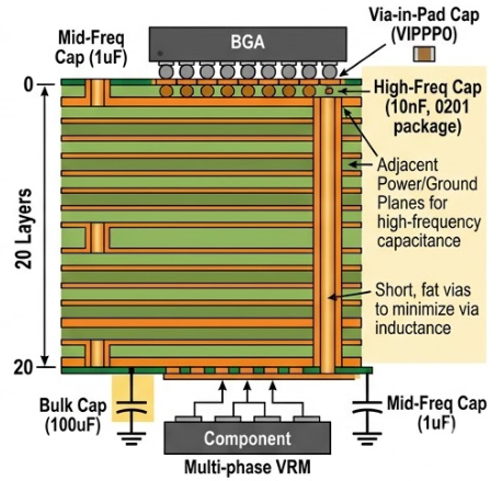
Power Delivery Network (PDN) Design for SerDes Stability
High-speed SerDes blocks (PLLs and Clock Data Recovery circuits) on high-speed digital PCBs are exquisitely sensitive to power supply noise. A noisy power rail translates directly into RJ (Random Jitter) and DJ (Deterministic Jitter) on the output eye.
Target Impedance Reduction on High-Speed Digital PCBs
The PDN on high-speed digital PCBs must maintain a low impedance across a wide frequency range.
- Decoupling Strategy for High-Speed Digital PCBs: Use a multi-phase voltage regulator module (VRM) combined with a hierarchy of decoupling capacitors:
- Bulk Capacitance (100uF-330uF): Handles VRM transient response on high-speed digital PCBs.
- Mid-Frequency (1uF-0.1uF): Handles board-level resonance on high-speed digital PCBs.
- High-Frequency (10nF-100pF): Placed directly under the BGA ball or on the opposite side of high-speed digital PCBs using small-package (0201) low-inductance capacitors.
Plane Resonance and Loop Inductance on High-Speed Digital PCBs
- Plane Spacing: Tight coupling between Power and Ground planes (e.g., 2-3 mil dielectric thickness) on high-speed digital PCBs creates excellent high-frequency inter-plane capacitance.
- Via Inductance: The loop area between the BGA ball, the via down to the decoupling cap, and the via back to the ground plane is the “killer” of PDN performance on high-speed digital PCBs. Short, fat vias (or via-in-pad) are mandatory for SerDes power integrity.
Navigating the Frontier: 112G and 224G PAM4 Design Constraints
The migration from NRZ (two voltage levels) to PAM4 (four voltage levels) on high-speed digital PCBs doubled the SerDes data rate in the same bandwidth, but it came at a -9.5 dB SNR penalty.
Insertion Loss Budget for 224G PAM4 SerDes
- Pre-FEC BER: The SerDes system on high-speed digital PCBs is designed to operate with a Bit Error Rate before Forward Error Correction that is significantly higher than older systems (e.g., 1e-5 pre-FEC).
- Channel Reach: A traditional 112G PAM4 SerDes channel on high-speed digital PCBs might tolerate 30 dB of insertion loss at Nyquist. For 224G PAM4 SerDes, the loss budget shrinks dramatically. This forces the use of Ultra-Low Loss materials and cabled backplane solutions or Co-Packaged Optics (CPO) for reach greater than a few inches on high-speed digital PCBs.
Managing Return Loss (S11) on High-Speed Digital PCBs
At 112G and above, reflections from S11 on high-speed digital PCBs can bounce between the transmitter package and the first PCB via, creating intersymbol interference (ISI) that spans multiple unit intervals.
- Requirement for High-Speed Digital PCBs: The via/connector launch on high-speed digital PCBs must exhibit an S11 better than -20 dB at Nyquist for robust SerDes operation.
Simulation, S-Parameters, and Verification Methodologies
“Guess and check” is not viable at 25 Gbps and above for high-speed digital PCBs. All SerDes designs must be validated in the virtual domain first.
The Simulation Flow for High-Speed Digital PCBs
- 2D Field Solver: Tools like Ansys HFSS or Keysight ADS are used to extract precise S-Parameter models for vias, connectors, and transmission line segments on high-speed digital PCBs. TI specifically cites the use of Ansys HFSS for modeling FPD-Link coax channels.
- 3D EM Simulation: For complex structures like BGA breakouts and connector launches on high-speed digital PCBs, a full 3D electromagnetic simulation is required to account for cross-coupling and resonance.
- Channel Simulation (IBIS-AMI): The extracted PCB S-Parameter file from high-speed digital PCBs is combined with IBIS-AMI models of the SerDes Tx/Rx. This simulates the Equalization (FFE, CTLE, DFE) and produces an Eye Diagram and Bathtub Curve.
Compliance Testing for High-Speed Digital PCBs
Before release to fabrication, the SerDes channel on high-speed digital PCBs must pass COM (Channel Operating Margin) analysis as defined by IEEE 802.3 standards. This metric calculates the signal-to-noise ratio budget and verifies that the physical high-speed digital PCBs channel is capable of supporting the targeted SerDes data rate.
Design for Manufacturability (DFM) in High-Speed Digital PCBs
Even a perfectly simulated high-speed digital PCBs design fails if it cannot be fabricated with high yield.
Etch Factor and Trace Width on High-Speed Digital PCBs
The etching process undercuts the copper on high-speed digital PCBs. For 3-4 mil traces, the final trace shape is trapezoidal. Sierra Circuits emphasizes working closely with the fabricator of high-speed digital PCBs to ensure that the Final Finished Trace Width matches the value used in the 2D field solver for impedance calculation.
Layer Registration for High-Speed Digital PCBs
Misregistration between layers on high-speed digital PCBs shifts the coupling between the SerDes signal trace and the reference plane. This is catastrophic for differential impedance. For HDI designs with microvias on high-speed digital PCBs, Class C or D registration tolerance is required.
Via Fill and Plating on High-Speed Digital PCBs
- Via-in-Pad (VIP): Essential for high-density BGA fanout on high-speed digital PCBs. VIP must be filled with a non-conductive epoxy and plated over (VIPPO) to prevent solder wicking away from the BGA ball during reflow. This ensures a flat, reliable SMT pad for SerDes components on high-speed digital PCBs.
Conclusion: The Integrated Design Flow
Designing high-speed digital PCBs is a multidisciplinary exercise that spans physics, materials science, and advanced manufacturing.
- Start with the Stackup and Materials: Define the Df threshold for high-speed digital PCBs based on your target SerDes data rate (e.g., Df < 0.004 for 112G PAM4).
- Simulate the Discontinuities: Use 3D solvers to model vias and connectors on high-speed digital PCBs, targeting S11 < -20 dB.
- Route with Precision: Follow differential routing rules on high-speed digital PCBs with strict P/N length matching, but do not fear 45-degree corners; fear via stubs and fiber weave.
- Optimize Power: Design a low-inductance PDN path on high-speed digital PCBs to keep PLL jitter to a minimum.
- Collaborate with the Fabricator: Engage the high-speed digital PCBs manufacturer early to align on trace width adjustments, backdrilling depth capabilities, and material availability.
By integrating the rigorous component-level guidelines from semiconductor vendors, the process-oriented manufacturing rules from fabrication experts, and the system-level simulation workflows from EDA platforms, designers can confidently navigate the challenges of 25 Gbps to 224 Gbps SerDes signaling and deliver robust, high-yield high-speed digital PCBs products for the AI and data center era.
Frequently Asked Questions (FAQ) on High-Speed Digital PCBs
Q1: What is the most critical factor for Signal Integrity in high-speed digital PCBs?
The most critical factor for Signal Integrity in high-speed digital PCBs is managing impedance discontinuities, particularly at vias and connectors, coupled with selecting laminates with a Dissipation Factor (Df) appropriate for the SerDes data rate. Without proper via backdrilling and material selection, even the best silicon cannot compensate for a poor high-speed digital PCBs channel.
Q2: How does PAM4 differ from NRZ in high-speed digital PCBs design?
In high-speed digital PCBs, PAM4 SerDes signaling doubles the data rate in the same bandwidth compared to NRZ, but it incurs a -9.5 dB SNR penalty. This makes the high-speed digital PCBs channel much more sensitive to insertion loss, reflections, and crosstalk. Consequently, PAM4 designs demand tighter impedance control and lower-loss laminates than equivalent NRZ high-speed digital PCBs.
Q3: Why is backdrilling essential for high-speed digital PCBs?
Backdrilling is essential on high-speed digital PCBs because via stubs create resonant nulls that can completely eliminate SerDes signal energy at the Nyquist frequency, destroying Signal Integrity. On high-speed digital PCBs operating above 10 Gbps, an un-backdrilled via stub acts as an open-circuit stub filter, rendering the channel unusable.
Q4: What laminate materials are recommended for 224G PAM4 high-speed digital PCBs?
For 224G SerDes links on high-speed digital PCBs, Ultra-Low Loss laminates with Df values between 0.0015 and 0.0025 are mandatory. Materials such as Megtron 8, Tachyon 100G, or Astra MT77 are typically specified for these high-speed digital PCBs to meet the extremely short channel reach budgets imposed by 224G PAM4 signaling.