mmWave PCB design for 77GHz radar and 5G high-frequency boards demands a paradigm shift from conventional low-frequency methods. This comprehensive guide consolidates authoritative insights from industry-leading sources, covering material selection, stack-up, layout, simulation, and manufacturing challenges to help engineers and procurement specialists achieve reliable, high-performance outcomes.
1. Core Material Selection for mmWave PCBs
1.1 Dielectric Constant (Dk) and Dissipation Factor (Df)
At mmWave frequencies, the PCB substrate’s electrical properties dominate performance. The two critical parameters are:
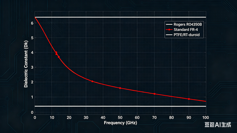
- Dielectric Constant (Dk): Must be tightly controlled and consistent across the board. Variations in Dk cause impedance mismatches, signal reflections, and phase errors. For 77 GHz radar, even a 1% Dk variation can shift antenna resonance by hundreds of MHz.
- Dissipation Factor (Df): Represents signal loss within the substrate. Low Df materials (e.g., 0.001–0.003) are mandatory to minimize attenuation. High Df materials (common in FR-4) cause excessive heating and signal degradation at mmWave.
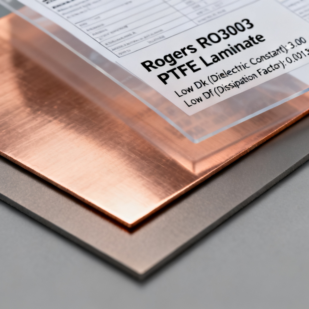
Recommended Materials:
- PTFE-based composites (e.g., Rogers RO3003, RO4350B, TMM series): Offer low Df (0.001–0.002) and stable Dk over temperature. RO3003 is a top choice for 77 GHz radar due to its extremely low loss and tight Dk tolerance (±0.04).
- Hydrocarbon ceramic laminates (e.g., Rogers 4350B, Isola Astra MT77): Balance cost and performance for 5G sub-6 GHz and mid-band mmWave. Astra MT77 excels in thermal stability for power amplifiers.
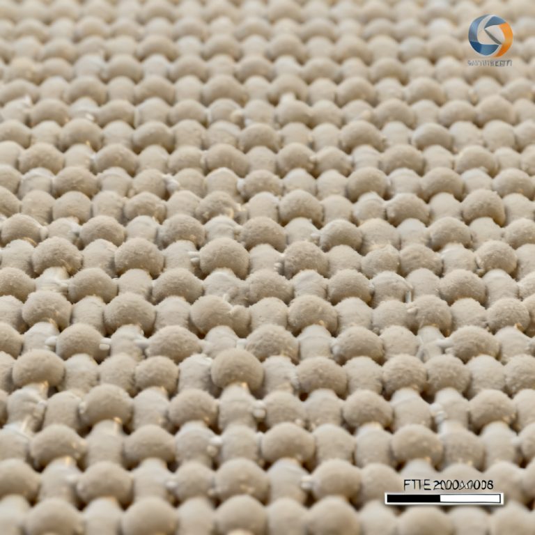
- LCP (Liquid Crystal Polymer): Suitable for flexible mmWave circuits, offering low moisture absorption and stable Dk up to 110 GHz.
Exclusion: Avoid FR-4 entirely above 1 GHz. Its high Df (0.02+) and uncontrolled Dk make it unusable for mmWave PCB design for 77 GHz or 5G mmWave.
1.2 Thermal Management
High-frequency power amplifiers in 5G and radar modules generate significant heat. Substrates must have high thermal conductivity (W/m·K). Materials like Rogers 4350B (0.62 W/m·K) or ceramic-filled PTFE (1.5 W/m·K) are preferred. For extreme heat, metal-core PCBs (MCPCB) with aluminum or copper base plates are used, though they require careful impedance control.
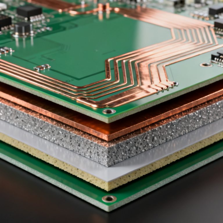
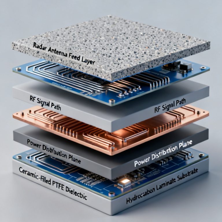
2. Stack-Up and Impedance Control
2.1 Stack-Up Design for 77 GHz and 5G
A typical mmWave stack-up uses a symmetric, multi-layer structure with dedicated layers for RF signals, power, and ground.
Critical Rules:
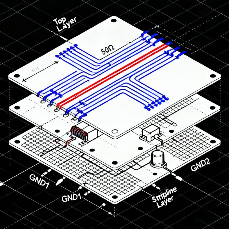
- Signal Layer: Use the top or bottom layer for critical RF traces to minimize via stubs and parasitic inductance.
- Ground Plane: Place a solid, continuous ground plane directly beneath the RF layer (ideally one layer below) to ensure controlled impedance. Avoid gaps or slots.
- Dielectric Thickness: For 77 GHz, the substrate height (h) between the signal trace and ground must be thin (e.g., 5–10 mils) to achieve 50-ohm impedance with reasonable trace widths (e.g., 8–12 mils). Thicker substrates require wider traces, increasing radiation losses.
- Prepreg vs. Core: Use low-loss prepreg (e.g., Rogers 2929 bondply) for bonding layers. Avoid standard FR-4 prepreg in the stack-up.
Example Stack-Up (4-layer, 77 GHz):
| Layer | Material | Thickness | Copper Weight |
|---|---|---|---|
| Layer 1 (Top): RF Signal (Microstrip) | Rogers RO3003 | 5 mil | 0.5 oz |
| Layer 2: Ground Plane | Rogers RO3003 | 5 mil | 1 oz |
| Core | Rogers RO3003 | 10 mil | N/A |
| Layer 3: Power or Low-Speed Digital | Rogers RO3003 | 5 mil | 1 oz |
| Layer 4 (Bottom): Ground or Secondary RF | Rogers RO3003 | 5 mil | 0.5 oz |
2.2 Impedance Calculation
Use 2D field solvers (e.g., Ansys HFSS, Keysight ADS) to compute trace dimensions. For a 50-ohm microstrip on RO3003 (Dk=3.0, h=5 mil):
- Trace width ≈ 9.5 mils (assuming 0.5 oz copper, 1 oz/ft²).
- For differential pairs (e.g., 100 ohms), spacing must be tightly controlled.
Avoid: Relying on impedance calculators without accounting for copper roughness, which increases loss at mmWave.
3. Layout and Routing Techniques
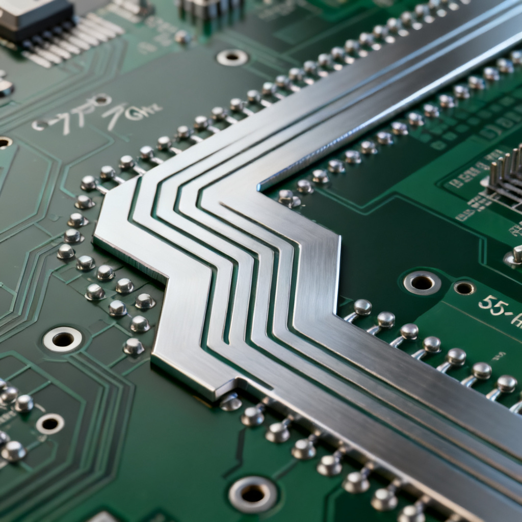
3.1 Trace Geometry and Routing
At 77 GHz (wavelength ~3.9 mm in air, ~1.3 mm on PCB), trace dimensions become comparable to wavelength. Key rules:
- Microstrip vs. Stripline: Microstrip is common for antenna feeds and short interconnects due to lower loss. Stripline is preferred for long runs to shield from external interference, but it has higher loss.
- Minimize Trace Length: Keep RF traces as short as possible. Every 1 mm of trace adds ~0.1 dB loss at 77 GHz on low-loss substrates.
- Avoid 90° Corners: Use 45° chamfered or curved bends. Right-angle bends cause impedance discontinuities and reflections.
- Via Stubs: Remove via stubs (back-drilling) for transitions between layers. A 10-mil stub at 77 GHz acts as an open circuit, causing severe resonance.
- Ground Vias: Place ground vias around RF traces (e.g., every λ/20, ~0.2 mm at 77 GHz) to suppress parallel-plate modes and cavity resonances.
3.2 Component Placement
- Antenna Feed: Place the antenna (patch, dipole, or array) directly on the same layer as the RF chip to avoid long feedlines.
- Decoupling Capacitors: Use high-frequency capacitors (e.g., 100 pF, 10 pF, 1 pF in parallel) placed as close as possible to power pins of active components.
- Isolation: Keep digital and analog/RF sections physically separate. Use guard rings or grounded walls (via fences) around sensitive RF blocks.
4. Simulation and Validation
4.1 Electromagnetic (EM) Simulation
Full-wave 3D EM simulation is non-negotiable for mmWave PCBs. Tools like Ansys HFSS, CST Microwave Studio, or Keysight Momentum model parasitic effects, radiation, and coupling.
Critical Simulations:
- S-Parameters: Verify insertion loss (S21) and return loss (S11) for all RF paths. Target S11 < -15 dB across the frequency band.
- Antenna Pattern: For 77 GHz radar, simulate the antenna gain, beamwidth, and side-lobe levels. Use infinite array boundary conditions for phased arrays.
- Crosstalk: Simulate coupling between adjacent traces. At 77 GHz, even 0.5 mm spacing may cause -20 dB coupling.
4.2 Manufacturing Tolerances
PCB fabrication introduces tolerances in etch, lamination, and drilling. For mmWave PCB design:
- Etch Tolerance: ±0.5 mil for trace width. This can shift impedance by 2–3 ohms.
- Dielectric Thickness: ±1 mil variation. Use controlled impedance testing (TDR) on coupons.
- Copper Roughness: Roughened copper (for adhesion) increases conductor loss. Specify “smooth copper” (e.g., electrodeposited with low profile) for RF layers.
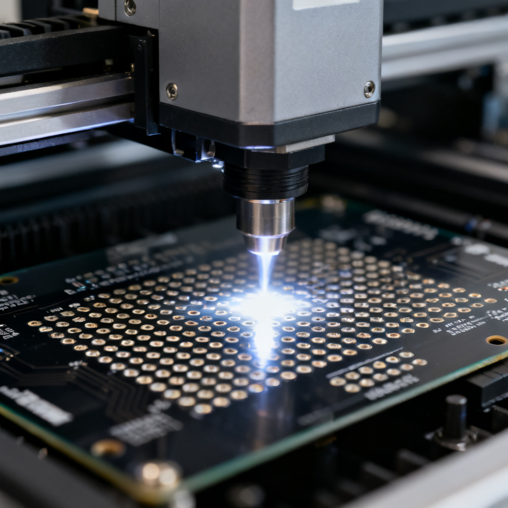
5. Manufacturing Challenges and Solutions
5.1 Plasma Treatment and Surface Finish
- Plasma Etching: Before lamination, treat PTFE surfaces with plasma (oxygen/argon) to improve adhesion without damaging the dielectric.
- Surface Finish: Use ENIG (Electroless Nickel Immersion Gold) for good solderability and flatness. Avoid HASL (Hot Air Solder Leveling) due to uneven surface causing impedance variation.
5.2 Drilling and Registration
- Via Diameter: For 77 GHz, use microvias (≤0.2 mm) with laser drilling to minimize parasitic inductance.
- Registration: Maintain ±1 mil alignment between layers. Misalignment causes impedance mismatch in differential pairs and antenna arrays.
5.3 Testing and Inspection
- Time-Domain Reflectometry (TDR): Measure impedance of each layer.
- Vector Network Analyzer (VNA): Test S-parameters on production boards.
- X-Ray Inspection: Verify via integrity and layer alignment.
6. Special Considerations for 77 GHz Radar
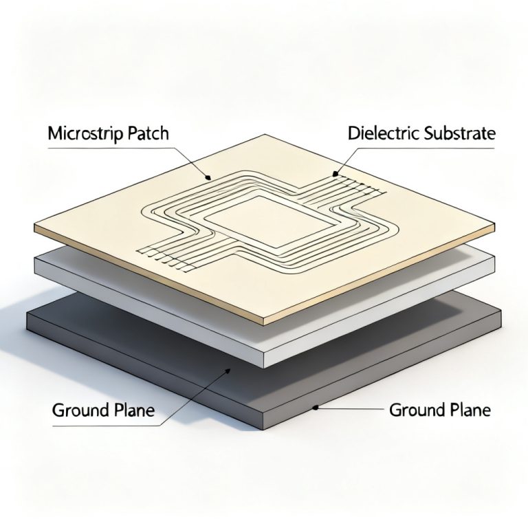
6.1 Antenna Array Design
- Patch Antennas: Use series-fed or corporate-fed microstrip patch arrays. For 77 GHz, a 4×4 array (16 elements) achieves ~15 dBi gain.
- Substrate Thickness: For patch antennas, substrate height should be ~0.01λ (0.13 mm at 77 GHz) to maximize bandwidth while suppressing surface waves.
- Grating Lobes: Ensure element spacing < λ/2 (1.95 mm at 77 GHz) to avoid grating lobes in phased arrays.
6.2 Waveguide Transitions
Many 77 GHz radar modules use waveguide (WR-10) interfaces. Design a microstrip-to-waveguide transition using a tapered slot or probe feed. Simulate the transition to achieve < -20 dB return loss.
7. Special Considerations for 5G High-Frequency Boards
7.1 Frequency Bands
- Sub-6 GHz (n77, n78, n79): Use materials like Rogers 4350B or Isola 370HR. Stack-up is less critical.
- mmWave (n260, n261 – 24–40 GHz): Use PTFE or LCP. Follow 77 GHz guidelines but with relaxed tolerances (e.g., trace width tolerance ±1 mil).
7.2 Power Handling
5G base stations require high power (up to 10W per channel). Use thick copper (2 oz or more) for power layers and ensure adequate thermal vias under power amplifiers.
FAQ: mmWave PCB Design for 77GHz Radar & 5G High-Frequency Boards
What is the most critical factor in mmWave PCB design for 77GHz radar?
The most critical factor is material selection. Using a substrate with a low and stable dielectric constant (Dk) and a very low dissipation factor (Df), such as Rogers RO3003, is essential to minimize signal loss and maintain impedance control at 77 GHz.
Can standard FR-4 be used for 5G high-frequency boards?
No. Standard FR-4 has a high dissipation factor (Df > 0.02) and uncontrolled Dk, making it unsuitable for any mmWave application, including 5G high-frequency boards. Low-loss materials like PTFE or hydrocarbon ceramic laminates are required.
How do I ensure impedance control for 77 GHz radar PCBs?
Impedance control is achieved through precise stack-up design, using thin dielectrics (e.g., 5 mils), tight trace width tolerances, and 2D field solvers for calculation. Manufacturing tolerances must be verified with TDR testing.
What simulation tools are recommended for mmWave PCB design?
Industry-standard tools include Ansys HFSS, CST Microwave Studio, and Keysight ADS. These full-wave 3D EM simulators can model parasitic effects, antenna patterns, and crosstalk at mmWave frequencies.
What are the key differences between designing for 77 GHz radar vs. 5G mmWave?
77 GHz radar requires even tighter tolerances (e.g., ±0.5 mil trace width) and thinner substrates (5–10 mils) due to the higher frequency. 5G mmWave (24–40 GHz) has slightly relaxed tolerances but still demands low-loss materials and careful layout. Both require rigorous simulation and manufacturing control.
“`