In the demanding world of power electronics—electric vehicle charging stations, industrial motor drives, and renewable energy inverters—traditional printed circuit boards often hit a physical limit. As currents exceed 50, 100, or even 200 amps, standard boards can fall victim to their own success, generating debilitating heat that leads to performance degradation or outright failure.[reference:0] This is the domain where heavy copper PCBs, typically defined as boards with copper weights ≥3oz/ft², transform from simple interconnects into critical “energy arteries” that ensure efficiency and longevity.[reference:1] This comprehensive guide navigates the intricate relationship between high-reliability design, extreme power handling, and advanced thermal management, exploring why merely increasing copper weight is not enough—and how a holistic, physics-driven strategy from trace geometry to system-level cooling is the key to unlocking robust, export-ready electronics.
Understanding Heavy Copper: Benchmarking Reliability and Performance
To engineer for reliability, one must first understand the fundamental physics that differentiate heavy copper circuits from their standard counterparts. The definition itself sets the stage: while a standard PCB might use 1oz or 2oz copper, a heavy copper board begins at 3oz, with high-end designs reaching up to 20oz or even 30oz per square foot.[reference:2][reference:3] This isn’t just a quantitative change; it’s a qualitative leap in capability.
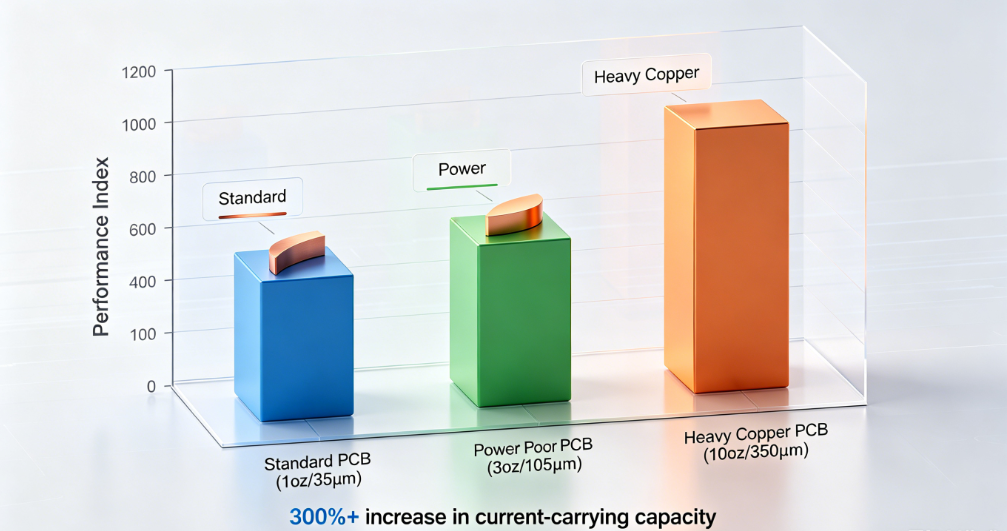
The core advantage lies in a simple electrical principle: thicker copper lowers resistance per unit length exponentially. A trace that measures a certain resistance in 1oz format can drop to a quarter or less of that value when rendered in 4oz or 6oz copper, subsequently minimizing I²R (Joule) heating.[reference:4] However, the benefits extend well beyond basic conductivity into structural integrity. Heavy copper plating acts as a reinforcing skeleton, increasing typical flexural strength by approximately 30% and vibration resistance by around 25%. This mechanical robustness is paramount for automotive and aerospace applications subjected to constant mechanical stress.[reference:5] The boards therefore excel in three interlocking performance pillars: high current capacity with minimal voltage drop, enhanced thermal dissipation that reduces heat buildup, and mechanical strength that resists warping and cracking under thermal cycling.[reference:6]
The Thermal Challenge: When High Power Creates High Risk
The very property that makes heavy copper desirable—its ability to channel massive currents—creates its most formidable engineering adversary: thermal management. Without a meticulously planned thermal strategy, a heavy copper board cannot achieve its potential for high reliability. Understanding these thermal nuances is the foundation upon which all successful high-power designs are built.
Anatomy of Heat Generation
Heat in a heavy copper PCB is not an external nuisance but an intrinsic byproduct of its operation. As current flows through even the highly conductive copper traces, resistive losses generate heat, a phenomenon mathematically described by Joule’s First Law: P = I²R (Power dissipated = Current squared × Resistance). In high-power applications with currents rising above 50A, even copper’s exceedingly low resistance can produce temperature elevations of 30°C or more above ambient levels if left unmanaged.[reference:7] Simultaneously, the power semiconductors themselves—MOSFETs, IGBTs, and GaN devices—concentrate heat in very small areas, with power densities peaking beyond 100W/cm² at the die level.[reference:8] This localized heat, when combined with background I²R losses, creates a compounding effect that accelerates material degradation processes like electromigration in conductors and dielectric breakdown in substrates.
Thermal Expansion, Mechanical Stress, and Failure Modes
Beyond absolute temperature rise, the dynamic mechanical stress of repeated heating and cooling cycles poses an equally grave threat to longevity. A PCB is a composite of disparate materials, each with its own Coefficient of Thermal Expansion (CTE). Copper expands at approximately 17 ppm/°C, while a common substrate like FR-4 has a CTE in the range of 14-18 ppm/°C.[reference:9] This CTE mismatch may seem small on paper, but over thousands of thermal cycles—from cold startup to full-load operation at elevated temperatures—the cumulative stress creates shearing forces at the interface between the copper barrel of a plated through-hole and the resin-rich substrate. The consequences are progressive and severe: barrel cracking (which breaks electrical continuity), pad cratering, and ultimately, catastrophic delamination that tears apart the internal layers of the board.[reference:10] In compact, high-density designs, these effects are magnified as heat becomes trapped, creating hot spots near power components where localized temperatures can exceed 100°C, leading to thermal runaway conditions or solder joint failure.[reference:11] This underscores why thermal management, from the very first design step, is non-negotiable for high-reliability applications.
Gold-Standard Design Rules for High-Reliability Power
Turning the knowledge of these challenges into a reliable physical product requires adhering to a disciplined set of design rules that optimize every micrometer of copper for both electronic and thermal performance. The following strategies constitute a framework for building failure-resistant boards.
Scientific Copper Weight Selection and Current Capacity
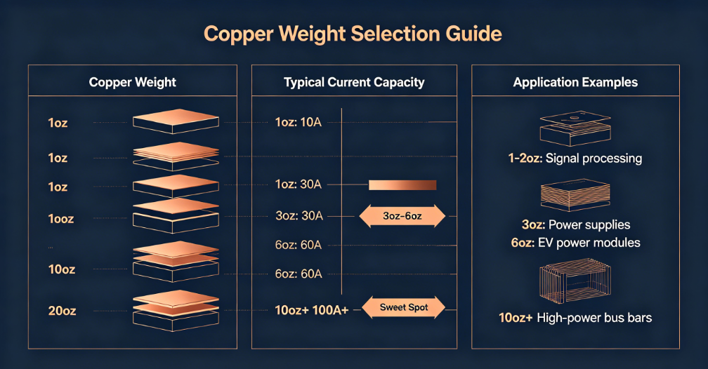
Selecting copper thickness is a decision of precision, not guesswork. The guiding principle must be “Current-Driven, Precision Matching,” actively rejecting the misconception that thicker copper universally equates to a better board. Indiscriminately increasing copper weight drives up fabrication cost and, more critically, introduces manufacturing risks such as uneven etching and soldering defects due to massive thermal sinking during assembly.[reference:12]
For a reliable starting point, a practical rule of thumb for estimating current capacity under moderate ambient conditions (≤40°C) is: Current (A) ≈ Copper Thickness (oz) × Trace Width (mm) × 0.8. This provides a rapid sanity check, but for precise engineering, designs must be validated against the IPC-2221 generic standard on printed board design, which dictates the precise relationship between conductor sizing, current, and acceptable temperature rise. Real-world examples with 3oz copper demonstrate a 3mm wide trace can comfortably handle approximately 7.2A, sufficient for many industrial power supply applications. Industry engineering advice converges on a sweet spot: prioritize mainstream specifications between 3oz and 6oz for most high-reliability applications, reserving designs above 10oz only when strictly required by the physics (e.g., certain aerospace bus bars), as this “risk zone” introduces significant challenges with board warping and drilling reliability.[reference:13]
Trace Geometry and Layout Optimization
Once copper weight is chosen, the physical shape of every trace becomes a critical variable. Large currents require carefully specified minimum widths, which escalate rapidly with copper thickness. For 3oz copper, minimum trace width should be no less than 0.3mm, while a conductor carrying 10A on 6oz copper necessitates a width of at least 5mm to avoid resistive heating. Beyond static width, trace transitions are a classic failure origination point. Abrupt neck-downs, where a wide trace suddenly narrows, act as “current bottlenecks,” concentrating ohmic heating at a single point. Every such transition must instead use a tapered slope, with a transition length equal to or greater than three times the width difference between the two connecting segments. At the layout level, thermal optimization involves leveraging large unbroken copper pours that are connected to ground and power planes through dense thermal via structures, which turns the entire board volume into a distributed heat exchanger.[reference:14]
Via Architecture for Power Delivery and Heat Transfer
Vias in heavy copper designs serve a dual, life-or-death function: conducting hundreds of amps vertically between layers and shunting heat away from hot surface-mounted devices. The manufacturing process demands specific geometric limits to ensure a reliable plated barrel. For 3oz copper, a minimum drill diameter of 0.8mm is required to guarantee uniform plating; for 6oz and above, minimum diameter jumps to 1.0mm. Hole wall copper plating for heavy designs must reach a minimum of 25µm to withstand thermal cycling. For advanced thermal vias specifically, the function shifts to z-axis heat conduction, and here the optimal configuration is different: small-diameter vias (0.3-0.5mm) placed on a tight pitch of 0.8-1.2mm directly under high-power component pads. These dense via arrays create a high-conductivity “thermal pipe” that shunts heat into large internal ground planes or directly to a backside heatsink.[reference:15] For extreme cases, direct-fill copper thermal vias of millimeter-scale sizes can achieve heat transfer coefficients exceeding 3000 W/cm²·K, a leap beyond standard plated vias.[reference:16]
Advanced Thermal Management: Building a Superior Heat Flow Path
Designing a high-reliability board means engineering an optimized heat flow path from the semiconductor junction all the way out to the ambient environment. Understanding the hierarchical nature of this pathway allows designers to systematically eliminate thermal bottlenecks. Effective heavy copper PCB thermal management requires integrated approaches addressing material selection, copper weight distribution, via architecture, and heat spreading path optimization.[reference:17]
System-Level Heat Path Engineering
Successful thermal design can be visualized as a three-tiered highway system. At the component level, heat transfers from the tiny semiconductor junctions through die attach materials into the top-layer copper planes. At the board level, thermal energy spreads laterally along the heavy copper layers for redistribution while simultaneously moving vertically through thermal vias into inner power planes. At the system level, heat exits the board through the substrate to external cooling mechanisms like heatsinks or chassis. The critical design principle is that each interface in this chain represents a thermal resistance point that must be systematically minimized to prevent the formation of a bottleneck that chokes off the entire heat flow.[reference:18]
Copper Inlay and Embedded Coin Technology
When standard via arrays reach their physical limits in extracting heat from extreme power devices, advanced embedded structures provide the next evolutionary step. Copper coin technology embeds solid thick copper slugs—typically 1-3mm in thickness—directly into precisely routed cavities within the PCB stack-up. These solid copper masses create uninterrupted, low-resistance thermal highways from the component’s thermal pad straight through to an external heatsink or metal core, bypassing the higher-resistance laminate layers. The result is a measured reduction in total thermal resistance of 40-60% compared to even the best thermal via array, making such structures indispensable in the highest-tier power designs.[reference:19]
Advanced Substrates and External Cooling Integration
The base laminate itself can be a liability; the inherently poor thermal conductivity of standard FR-4 (a glass-reinforced epoxy with a thermal conductivity typically around 0.3-0.4 W/m·K) can be surmounted by switching to advanced substrates. For extreme environments, metal-core PCBs (MCPCBs), ceramic substrates (alumina or aluminum nitride), and high-Tg, low-CTE hydrocarbon laminates offer dramatically superior heat spreading. External cooling must be integrated into the design from the outset, not treated as an afterthought. Forced-air convection, strategic heatsink placement, and liquid cold-plate integration all see enhanced effectiveness when the internal heavy copper planes are structured to efficiently deliver heat to their point of transfer.[reference:20][reference:21]
Manufacturing Excellence: DFM for Heavy Copper Multilayers
A perfect design is only as good as the manufacturing process that realizes it. Heavy copper production requires specialized techniques that differ fundamentally from standard PCB fabrication. The value of a robust Design for Manufacturability (DFM) strategy lies in preemptively resolving the unique production challenges that arise when working with extreme copper weights. Manufacturers must transition away from standard etching and plating processes towards alternative manufacturing techniques that include step plating and differential etching.[reference:22]
Navigating Production Pitfalls
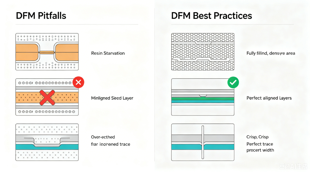
Manufacturing heavy copper multilayers introduces specific risks that designers must anticipate. While an increase in copper thickness from 1oz to 6oz yields proportionally higher current capacity, the diminishing returns that appear beyond 10oz are not merely electronic but mechanical and thermal in nature—the substrate’s thermal resistance becomes the dominant bottleneck, and mechanical stresses from CTE mismatch intensify.[reference:23] Common manufacturing defects include resin starvation gaps caused by uneven copper features, inner layer misregistration during lamination under high pressure, and over-etching of fine features due to the long dwell times required to etch thick base copper. Additional pitfalls involve the difficulty of adjusting differential etch factors between thick and adjacent thin copper in mixed-weight designs. Mitigating these requires close collaboration with manufacturing engineers to simplify layer stack-ups, ensure even copper distribution for resin flow, and build in proper etch compensation factors from the outset.[reference:24]
Plating, Etching, and Solder Mask Engineering
The core challenge in finishing heavy copper boards is managing the severe topography created by the thick circuitry. The extreme height difference between the base laminate surface and the top of a 10oz copper trace can exceed 350µm, creating an alpine landscape that solder mask cannot easily bridge. Without specialized techniques such as dam-and-fill solder mask application or the use of multiple mask coats, air entrapment at the trace edges leads to corrosion cells. Simultaneously, the electroplating process for through-holes must deliver sufficient current density to plate deep barrel walls without creating excessive surface buildup, a balance achieved through pulse plating and specialized bath chemistry. Post-etch inspection with Automated Optical Inspection (AOI) systems must be calibrated for the dimensional nuances of thick copper lines to avoid false callouts for acceptable etching profiles such as trapezoidal trace cross-sections, which are a natural feature of the etch process.[reference:25]
Quality Assurance and Testing for High-Reliability Compliance
Proving the reliability of a heavy copper board requires a validation regime far more exhaustive than simple continuity testing. Every board destined for the high-reliability field must undergo a battery of physical and environmental tests that simulate a lifetime of operational stress to screen for latent manufacturing defects. An integrated testing strategy is fundamental to a quality assurance program, ensuring the design matches electrical needs and can withstand extreme operational conditions.[reference:26]
Thermal Stress and Interconnect Reliability Testing
The true battleground for heavy copper reliability is the solder joint and plated through-hole barrel under thermal cycling stress. Thermal Shock Testing, in which boards are subjected to rapid air-to-air transitions between extreme temperatures (e.g., -40°C to +125°C) to simulate ambient shifts, is a primary screening tool. A more aggressive method, Interconnect Stress Testing (IST), passes a precisely controlled DC current through a daisy-chain network of vias and traces, heating them from within to a defined temperature (typically 150°C to 260°C) repeatedly to force failures at the weakest copper grain structures. Microsectioning of these stressed coupons then reveals the initial barrel cracks or corner defects that signal impending field failure, allowing for root-cause analysis and process refinement.
Thermal Imaging and Power Cycling for Design Validation
Beyond pass-fail tests, design validation requires quantifying the thermal performance of the entire board under live-load conditions. Infrared (IR) thermography captures a real-time, non-contact heat map of an operating board, visually identifying any unexpected hot spots, current crowding at trace corners, or uneven current sharing in parallel vias. Power cycling tests, which involve repeatedly ramping the board from zero load to full-rated power over thousands of cycles, collect data on the board’s thermal impedance over time. A rise in thermal impedance over successive cycles is a leading indicator of interface delamination between the copper barrel and the laminate, providing a quantitative measure of true field reliability and operational lifespan.
Application Frontiers: Electrification and Digital Infrastructure
The translation of these design and manufacturing principles into tangible products is most visible in the sectors driving global electrification. Heavy copper PCBs find their most critical deployment in high-current, high-reliability applications where failure is not an option, directly supporting trends in electrification and digital infrastructure.[reference:27]
In electric vehicle power modules, heavy copper boards form the backbone of motor inverters, on-board chargers, and battery management systems, channeling hundreds of amperes between the battery pack and traction motor with minimal losses—thermal performance directly dictating vehicle range and charging speed. The renewable energy sector depends on them for solar inverter circuits and wind turbine power converters, which must operate at full-rated power for decades through sandstorms, salt spray, and sub-zero temperatures. Meanwhile, the explosive growth of artificial intelligence and high-performance computing has pushed server power consumption into the kilowatts-per-rack range, meaning the baseboards delivering power to GPUs and ASICs demand heavy copper layers capable of managing extreme power density and heat dissipation while maintaining perfect voltage stability to prevent computational errors.[reference:28] This convergence of energy and data ensures that the principles of heavy copper thermal design, once a niche discipline, are now central to modern electronics engineering and the global high-tech supply chain.
Frequently Asked Questions
What defines a heavy copper PCB and why does it matter for high-power designs?
A heavy copper PCB is defined by having copper conductors weighing 3 ounces per square foot or more. This increased thickness provides several critical advantages: superior current-carrying capacity, significantly improved thermal management through better heat spreading, and enhanced mechanical strength that resists warping and cracking. These properties make heavy copper PCBs essential for applications like electric vehicle power modules and renewable energy converters, where reliability and minimal energy loss are critical. The fundamental difference from standard PCBs is an elevated thermal mass and spreading capability that prevents destructive hot spot formation.
How do I determine the right copper thickness for my application?
Selecting the appropriate copper thickness requires a “precision-matching” approach based on current requirements rather than simply choosing the thickest option. A practical engineering starting point is the estimation: Current Capacity (A) ≈ Copper Thickness (oz) × Trace Width (mm) × 0.8. For the majority of high-reliability industrial applications, 3oz to 6oz copper represents the optimal balance of performance, cost, and manufacturability. While specialized applications may require 10oz or more, thicknesses in this upper range introduce significant manufacturing complexities including board warping, uneven etching, and soldering difficulties. The IPC-2221 standard provides the authoritative reference for precise calculations based on your specific current and allowed temperature rise parameters.
What are the most effective thermal management strategies for heavy copper boards?
Effective heavy copper PCB thermal management demands a multi-layered strategy addressing material selection, copper weight distribution, via architecture, and heat spreading path optimization. The most impactful techniques include: optimized thermal via arrays directly beneath power components to create vertical heat paths; thick copper planes for lateral heat spreading; and copper coin technology for high-power devices, which embeds solid copper slugs into routed cavities to achieve a 40-60% reduction in thermal resistance compared to standard solutions. System-level integration with forced-air cooling, heat sinks, or liquid cooling must be planned from the earliest design stages.