In high-performance electronics, a Ceramic PCB Substrate like alumina or aluminum nitride is essential for managing extreme heat, high frequencies, and harsh environments. This guide explores every aspect of these materials to help you select the ideal substrate for your project.
Properties | Comparison | Applications | FAQ
Properties of Ceramic PCB Substrate: Alumina & Aluminum Nitride Boards
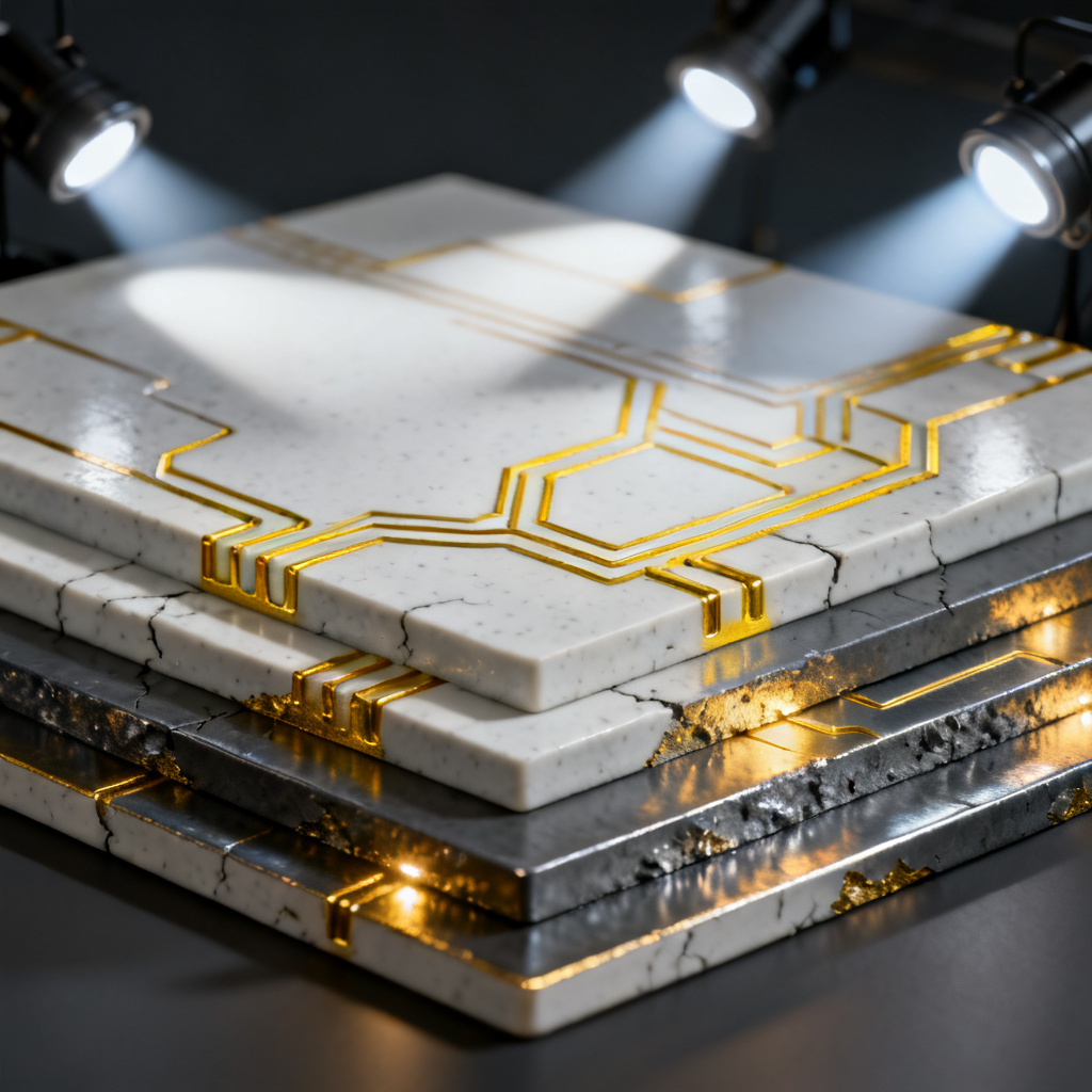
Ceramic PCB Substrate materials offer distinct properties that set them apart from traditional FR4. Alumina (Al₂O₃) provides a balance of thermal conductivity and cost-effectiveness, while aluminum nitride (AlN) excels in extreme thermal management. These ceramic PCB substrates feature high thermal conductivity, excellent electrical insulation, low coefficient of thermal expansion, and robust mechanical strength.
Alumina (Al₂O₃) Properties
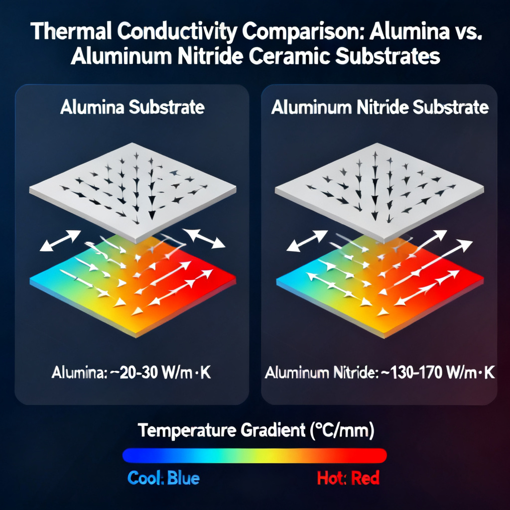
Alumina ceramic PCB substrate typically comes in 96% or 99.6% purity levels. Its thermal conductivity ranges from 20 to 30 W/mK, significantly higher than FR4. The dielectric constant is around 9.8 at 1 MHz, making it suitable for RF applications. With a dielectric strength of 10–15 kV/mm and CTE of 6–8 ppm/°C, alumina aligns well with silicon chips. It operates up to 1500°C, though practical limits are lower due to copper bonding.
Aluminum Nitride (AlN) Properties
Aluminum nitride ceramic PCB substrate boasts thermal conductivity of 170–200 W/mK, nearly ten times higher than alumina. Its dielectric constant is 8.8–9.0 at 1 MHz, with dielectric strength of 15–20 kV/mm. The CTE of 4.5–5.5 ppm/°C closely matches silicon, reducing thermal stress. AlN operates up to 1000°C in inert atmospheres and maintains excellent electrical insulation even at elevated temperatures.
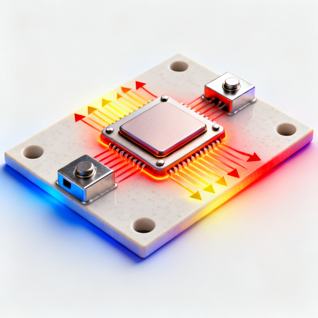
Advantages of Ceramic PCB Substrate for Thermal Management
Ceramic PCB Substrate materials provide superior thermal management compared to traditional substrates. They conduct heat away from components, reducing junction temperatures and improving reliability. AlN substrates can handle power densities up to 300 W/cm², while FR4 fails above 10 W/cm². This makes ceramic PCB substrates ideal for high-power LED arrays, power inverters, and RF power amplifiers.
High-Frequency Performance
Low dielectric loss and stable Dk over frequency make ceramic PCB Substrate materials ideal for RF and microwave circuits. Signal integrity is maintained up to 100 GHz, enabling applications in base station antennas, radar modules, and satellite communication systems. The low loss tangent ensures minimal signal degradation at high frequencies.
Mechanical and Environmental Resilience
Ceramic PCB Substrate resists moisture, chemicals, and UV radiation. They can operate in temperatures from -55°C to +300°C, with special designs handling even higher ranges. This resilience makes them suitable for automotive, aerospace, and industrial environments where reliability is critical.
Comparison Between Alumina and Aluminum Nitride Ceramic PCB Substrates
| Parameter | Alumina (Al₂O₃) Ceramic PCB Substrate | Aluminum Nitride (AlN) Ceramic PCB Substrate |
|---|---|---|
| Thermal Conductivity | 20–30 W/mK | 170–200 W/mK |
| Dielectric Constant (1 MHz) | 9.8 | 8.8–9.0 |
| CTE (ppm/°C) | 6–8 | 4.5–5.5 |
| Cost | Low | High |
| Typical Applications | General power, LED, RF | High-power, EV, laser |
| Brittleness | Moderate | Lower than alumina |
Applications of Ceramic PCB Substrates in Power Electronics
Ceramic PCB Substrate materials are widely used in power electronics for IGBT modules, DC-DC converters, and solid-state relays. Their high thermal conductivity ensures efficient heat dissipation, prolonging component life. In LED lighting, ceramic PCB substrates enable high-brightness LED arrays in streetlights and automotive headlights. For RF and microwave applications, these substrates support base station antennas, radar modules, and satellite communication systems.
Automotive and Aerospace Applications
Ceramic PCB Substrate is critical for battery management systems in electric vehicles, engine control units, and avionics. The low CTE and high thermal conductivity ensure reliability under thermal cycling. In medical electronics, ceramic PCB substrates are used in ultrasound transducers and laser surgical equipment, benefiting from their biocompatibility and chemical resistance.
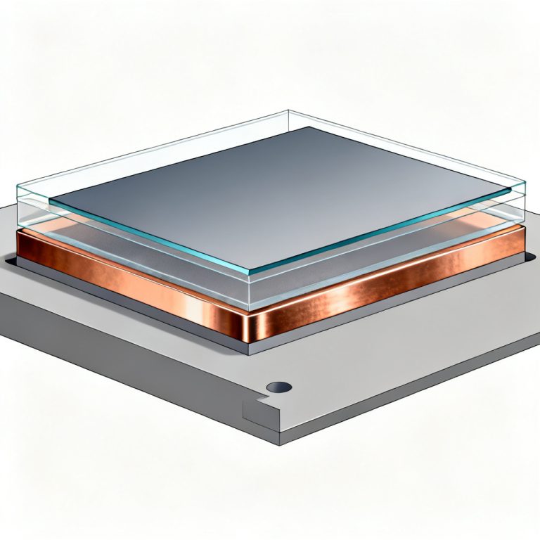
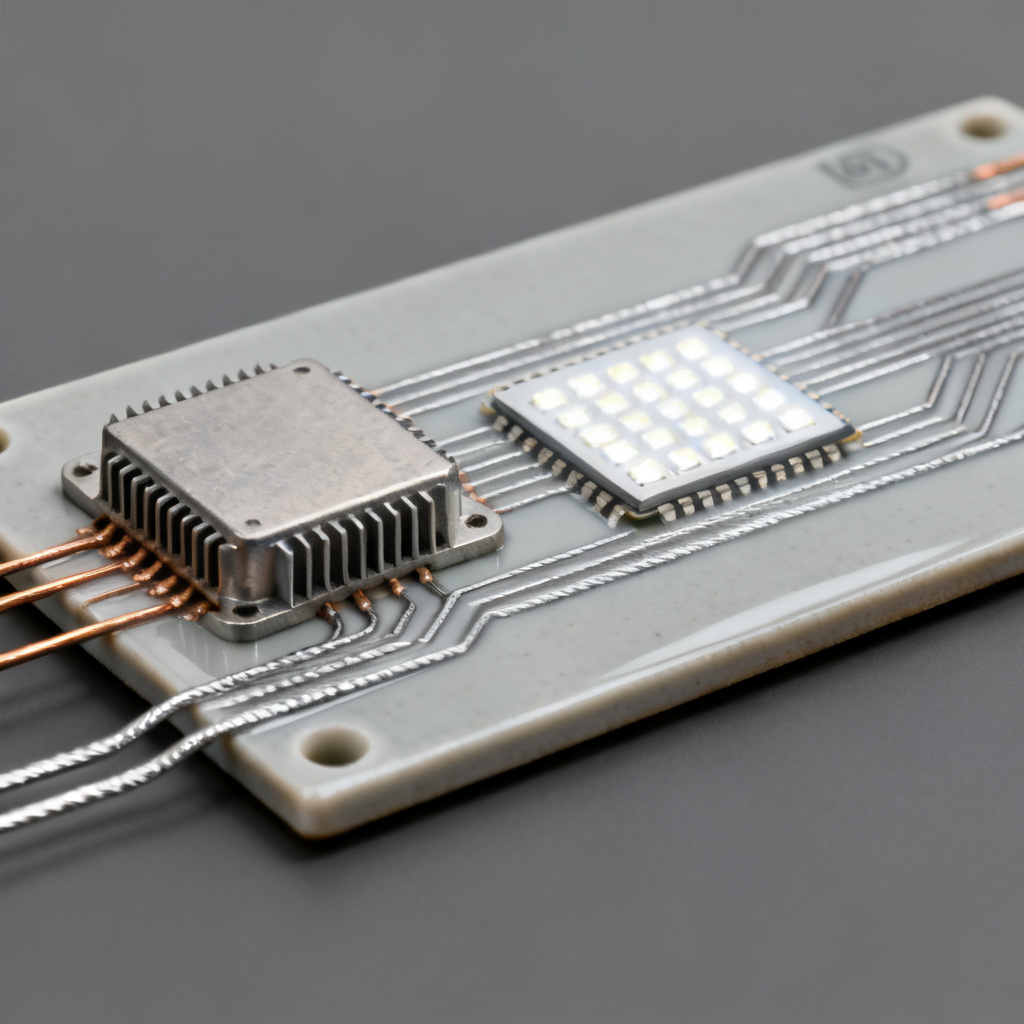
Manufacturing Process of Ceramic PCB Substrates
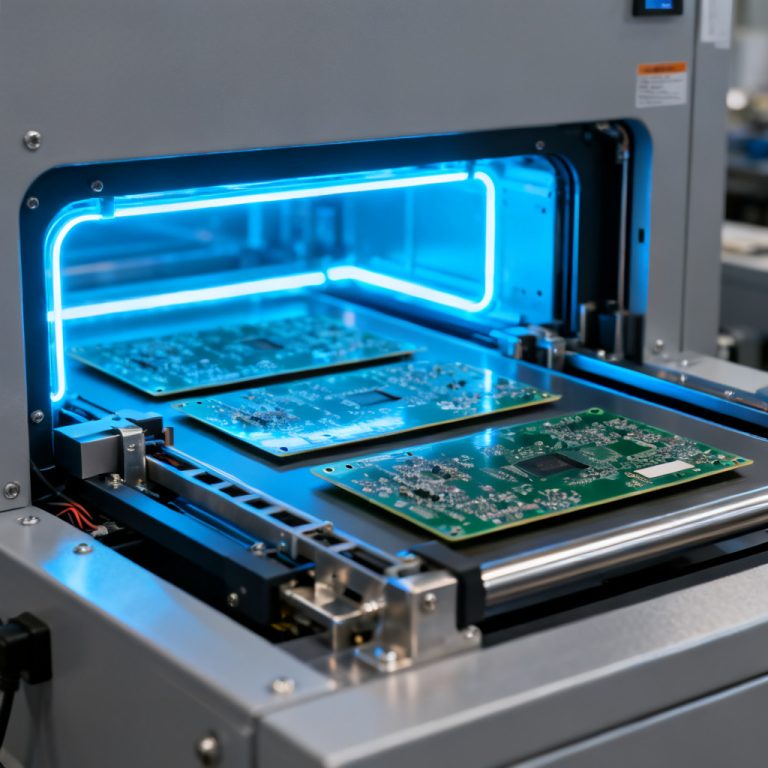
The production of Ceramic PCB Substrate involves tape casting, sintering, and metallization. Alumina or AlN powder is mixed with binders, cast into sheets, and fired at high temperatures. Direct Bond Copper (DBC) or Active Metal Brazing (AMB) bonds copper to the ceramic. Photolithography and etching create precise circuit patterns. Quality control includes thermal cycling, dielectric strength testing, and X-ray inspection to ensure reliability.
FAQ: Ceramic PCB Substrate: Alumina & Aluminum Nitride Boards
What is the main difference between alumina and aluminum nitride ceramic PCB substrates?
The main difference is thermal conductivity. Aluminum nitride ceramic PCB substrate offers 170–200 W/mK, while alumina provides 20–30 W/mK. AlN is better for extreme heat dissipation but costs more.
Can ceramic PCB substrates be used for high-frequency RF designs?
Yes, ceramic PCB substrate materials like alumina and AlN have low dielectric loss and stable Dk, making them ideal for RF and microwave circuits up to 100 GHz.
What are the cost considerations for choosing a ceramic PCB substrate?
Alumina ceramic PCB substrate is 3–5 times cheaper than aluminum nitride. For cost-sensitive applications with moderate thermal needs, alumina is preferred. For high-power density designs, AlN is necessary despite higher cost.
How does the CTE of ceramic PCB substrates affect component reliability?
The CTE of ceramic PCB substrate (6–8 ppm/°C for alumina, 4.5–5.5 ppm/°C for AlN) closely matches silicon (2.6 ppm/°C), reducing thermal stress during temperature cycling and improving solder joint reliability.
Professional Terminology in Ceramic PCB Substrate Technology
Dielectric Constant (Dk): A measure of a material’s ability to store electrical energy, critical for impedance control in RF designs. Coefficient of Thermal Expansion (CTE): The rate at which a material expands with temperature, important for matching to silicon. Direct Bond Copper (DBC): A process that bonds copper to ceramic at high temperature, creating a robust metallization layer. Active Metal Brazing (AMB): A technique using a brazing alloy to join copper to aluminum nitride, enabling high-reliability substrates. Thermal Conductivity: The ability to transfer heat, measured in W/mK; AlN’s high value makes it ideal for power modules.