Master the intricacies of SerDes PCB design for 56G/112G PAM4 high-speed routing. This guide covers loss budgets, stackup planning, via optimization, crosstalk control, and advanced techniques for next-gen high-speed interconnects.

The relentless demand for higher data throughput in data centers, 5G infrastructure, AI/ML accelerators, and high-performance computing has driven the industry from NRZ (Non-Return-to-Zero) signaling to PAM4 (Pulse Amplitude Modulation 4-level). At 56 Gbps and 112 Gbps, the challenges are immense. A single bit time is less than 18 picoseconds, and the voltage margin for PAM4 is one-third that of NRZ. This guide, compiled from the most authoritative sources in the industry, provides a complete playbook for designing PCBs that can reliably route these ultra-high-speed SerDes signals.
We will cover everything from fundamental channel loss budgets to advanced material selection, via optimization, and crosstalk management.
The Physics of PAM4 and the Channel Loss Budget in SerDes PCB Design
Before laying a single trace, you must understand the signal integrity (SI) physics. At 56G/112G PAM4, the channel is the enemy. This section explains the core physics behind SerDes PCB design for PAM4.
Why PAM4? The SNR Trade-off
Traditional NRZ signaling uses two voltage levels (0 and 1), requiring a high signal-to-noise ratio (SNR). PAM4 uses four voltage levels (00, 01, 11, 10), doubling the data rate per symbol. However, this comes at a cost: voltage margin is reduced by ~9.5 dB compared to NRZ, and the system is far more susceptible to noise, jitter, and reflections.
The Total Loss Budget (TLB) for 56G/112G PAM4
Every SerDes link has a defined total loss budget, typically specified by the chip vendor (e.g., 28-35 dB at Nyquist frequency for 112G PAM4). This budget must account for all losses from the transmitter (Tx) package to the receiver (Rx) package.
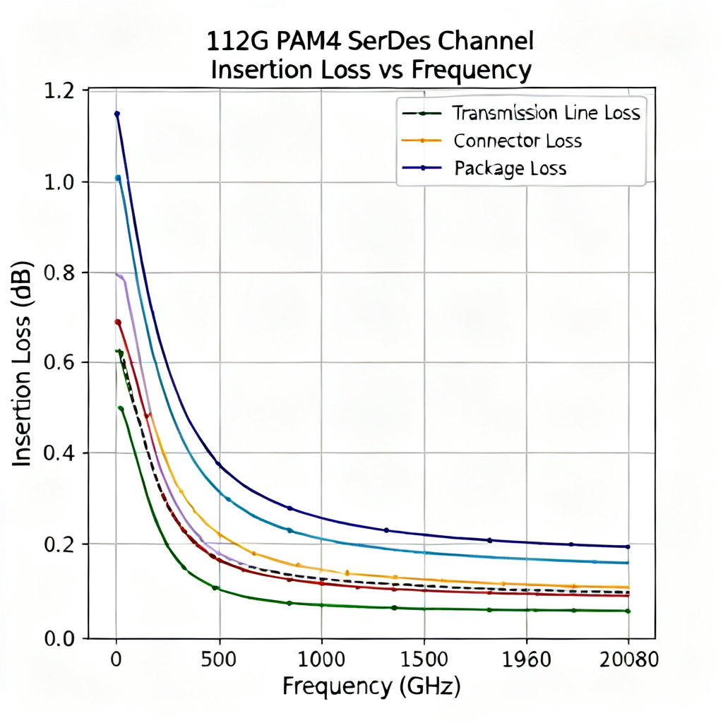
The key components of the loss budget are:
- PCB Trace Loss (Dominant): This is the largest controllable factor. It is a function of dielectric loss (Df), conductor loss (skin effect), and trace geometry. For 56G, standard FR4 is often insufficient. For 112G, you must use ultra-low-loss materials like Megtron 6/7/8, Isola Tachyon 100G, or Rogers 3000/4000 series. The Dissipation Factor (Df) should be < 0.005 at 10 GHz.
- Via Loss: A single via can introduce 0.5-1.5 dB of loss at 28 GHz. For a 112G link, a poorly designed via can consume 20-30% of the entire loss budget.
- Connector Loss: High-speed connectors have specified loss values.
- AC Coupling Capacitor Pad Loss: The pad capacitance creates an impedance discontinuity.
Actionable Rule of Thumb: For a 28 dB budget at 112G PAM4, you can typically allocate ~15-18 dB for PCB traces, ~5-8 dB for vias (backdrilled), and ~2-4 dB for connectors and AC caps.
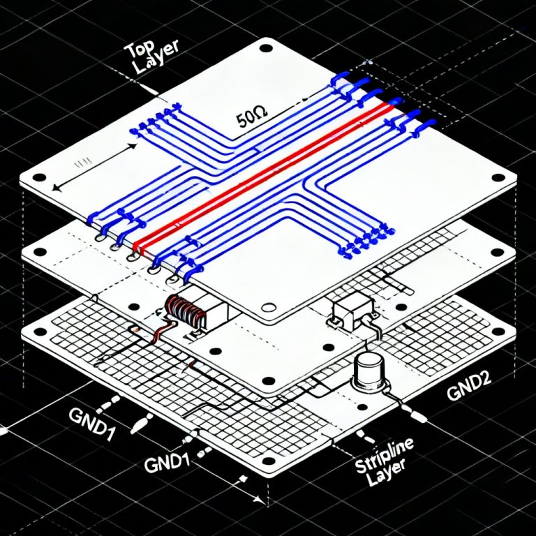
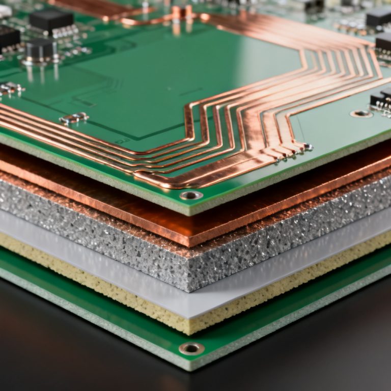
PCB Stackup and Material Selection for SerDes PCB Design
The stackup is the single most important design decision. It defines the impedance, loss, and manufacturability of your high-speed channels. This is a critical element of SerDes PCB design.
The “Thin Dielectric” Strategy
To achieve 100-ohm differential impedance with controlled trace widths (e.g., 6-8 mils), you must use thin dielectric cores between the signal layer and the adjacent reference plane. Typical core thickness is 4-5 mils (0.1-0.125 mm) for 112G. A thinner dielectric allows tighter coupling to the ground plane, reducing crosstalk.
The Ideal Stackup (Example 12-Layer)
A typical high-performance stackup for 56G/112G might look like this:
| Layer | Type | Purpose |
|---|---|---|
| Layer 1 (Top) | Signal (High-Speed) – Microstrip | Critical routing |
| Layer 2 | Ground Plane | Reference plane |
| Layer 3 | Signal (High-Speed) – Stripline | Shielded routing |
| Layer 4 | Power Plane | Power distribution |
| Layer 5 | Signal (General) | Low-speed signals |
| Layer 6 | Ground Plane | Reference plane |
| Layer 7 | Power Plane | Power distribution |
| Layer 8 | Signal (General) | Low-speed signals |
| Layer 9 | Ground Plane | Reference plane |
| Layer 10 | Signal (High-Speed) – Stripline | Shielded routing |
| Layer 11 | Ground Plane | Reference plane |
| Layer 12 (Bottom) | Signal (High-Speed) – Microstrip | Critical routing |
Key Rules: Every high-speed signal layer must be adjacent to a solid, unbroken ground plane. Use Stripline for the most critical 112G links. Avoid mixing 56G/112G signals with lower-speed control signals on the same layer.
Material Selection Checklist
| Material Grade | Df @ 10 GHz | Typical Use | Cost |
|---|---|---|---|
| Standard FR4 (e.g., 370HR) | 0.020 | Low-speed, < 10 Gbps | Low |
| Mid-Loss (e.g., Megtron 4) | 0.010 | 10-25 Gbps | Medium |
| Low-Loss (e.g., Megtron 6, Tachyon 100G) | 0.005 | 25-56 Gbps | High |
| Ultra-Low Loss (e.g., Megtron 7/8, Rogers 3000) | < 0.003 | 56-112 Gbps+ | Very High |
For 112G PAM4, use Megtron 7 or Tachyon 100G as a minimum. Cost is secondary to signal integrity.
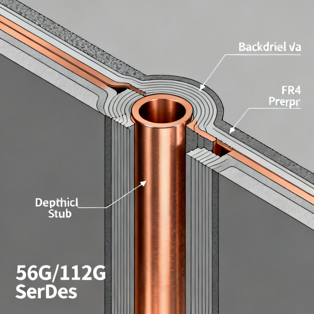
Via Optimization in SerDes PCB Design
Vias are the most common cause of failure in 56G/112G designs. This section covers via optimization for SerDes PCB design.
The Problem: The Stub
When a signal travels through a via, the unused portion of the via barrel (the “stub”) acts as a resonant cavity. At 28 GHz (Nyquist for 56G PAM4), a 40-mil stub can create a deep notch in the insertion loss (S21) at the resonant frequency.
The Solution: Backdrilling
Backdrilling is a controlled-depth drilling process that removes the via stub. The drill bit is larger than the original via hole and is designed to stop just short of the signal layer. For 56G, backdrilling is mandatory. For 112G, it is non-negotiable. The backdrill depth must be controlled to within ± 2-3 mils.
Advanced Via Optimization Techniques
- Microvias (HDI): For the most critical 112G links, use stacked microvias (laser-drilled) instead of through-hole vias.
- Via-in-Pad (VIP): Placing the via directly in the BGA pad minimizes the breakout length. This requires a non-conductive fill (e.g., epoxy) and copper capping.
- Anti-Pad Size: Make the anti-pad diameter 2-3 times the drill diameter to reduce capacitance.
- Grounded Via Fences: Surrounding a high-speed via with a ring of ground vias creates a coaxial-like structure.
Actionable Rule: For any via on a 56G/112G link, backdrill it to within 5 mils of the signal layer.
Routing Guidelines for PAM4 Signals in SerDes PCB Design
Routing at these speeds is about controlling impedance, minimizing discontinuities, and managing crosstalk. This is a core aspect of SerDes PCB design.
Differential Pair Routing
- Controlled Impedance: Target 100 ohms differential (±10%).
- Skew Matching: Match the length of the P and N traces within ± 2-3 mils (0.05-0.075 mm).
- Trace Gap: Keep the gap between the P and N traces constant.
- Bend Radius: Use 45-degree chamfered corners or curved bends with a radius of at least 3x the trace width.
Breakout Region (BGA Fanout)
- Layer Escalation: Use multiple layers to fan out the high-speed pairs.
- Dog-Bone vs. Via-in-Pad: For 112G, VIP is strongly preferred.
- Clearance: Maintain 2x trace width clearance between high-speed pairs in the breakout region.
AC Coupling Capacitors
- Placement: Place them as close to the transmitter as possible.
- Pad Size: Use the smallest pad size recommended by the capacitor manufacturer (e.g., 0402 or 0201).
- Ground Plane Cutout: Remove the ground plane directly under the capacitor pads.
Guard Traces and Grounding
- Guard Traces: Place a ground trace (with vias to ground at both ends) between adjacent high-speed pairs.
- Stitching Vias: Every high-speed signal trace should have a ground via within 50 mils of its start and end point.
Crosstalk and EMI Mitigation in SerDes PCB Design
At 56G/112G, crosstalk can close the eye completely. This section addresses crosstalk and EMI in SerDes PCB design.
Types of Crosstalk
- Near-End Crosstalk (NEXT): Noise coupled back to the transmitter on an adjacent quiet line.
- Far-End Crosstalk (FEXT): Noise coupled to the receiver on an adjacent quiet line. FEXT is the dominant problem for long, parallel traces.
The “3W” Rule and Beyond
The classic “3W” rule (3x trace width spacing) is insufficient for 112G PAM4. Recommended spacing: For stripline, maintain 5H spacing (where H is the distance from the signal layer to the nearest ground plane). For microstrip, use 10H.
Shielding Techniques
- Ground Planes: A solid, unbroken ground plane adjacent to the signal layer is the best shield.
- Co-Planar Waveguide: In microstrip, surround the signal trace with ground copper on the same layer.
EMI Control
- Slotted Ground Planes: Never route a high-speed signal over a slot in the ground plane.
- Ferrite Beads: Use ferrite beads on power supplies to high-speed ICs.
- Stitching Vias: Place ground vias every λ/20 (approximately 50-100 mils at 56G) along the edges of the PCB.
Simulation and Validation for SerDes PCB Design
No amount of rules can replace simulation. This section covers simulation and validation in SerDes PCB design.
Pre-Layout Simulation
- Channel Simulator: Use tools like Ansys HFSS, Keysight ADS, or Cadence Sigrity.
- S-Parameter Model: Obtain S-parameter models for your PCB material, connectors, and IC packages.
- Eye Diagram: Simulate the eye diagram at the receiver. The eye must be open at the specified BER (e.g., 1e-12).
Post-Layout Extraction
- Extract S-Parameters: After routing, extract the S-parameters of the entire channel.
- Time Domain Reflectometry (TDR): Simulate a TDR plot to identify impedance discontinuities.
Key Metrics to Verify
| Metric | Target Value |
|---|---|
| Insertion Loss (S21) | Within budget |
| Return Loss (S11) | < -15 dB |
| Crosstalk (S41, S31) | < -30 dB |
| Eye Height | > 50 mV (for 112G PAM4) |
| Eye Width | > 0.3 UI |
FAQ: SerDes PCB Design for 56G/112G PAM4
What is the most critical aspect of SerDes PCB design for 112G PAM4?
The most critical aspect of SerDes PCB design for 112G PAM4 is managing the total loss budget, particularly through material selection, via optimization, and controlled impedance routing.
Can I use standard FR4 for 56G PAM4 SerDes PCB design?
No, standard FR4 is insufficient for 56G PAM4 SerDes PCB design. You must use mid-loss or low-loss materials like Megtron 4 or Tachyon 100G to meet the loss budget.
Why is backdrilling essential in SerDes PCB design for 112G?
Backdrilling removes via stubs that cause resonant notches in insertion loss. In SerDes PCB design for 112G, backdrilling is non-negotiable to maintain signal integrity.
What is the recommended spacing for high-speed pairs in SerDes PCB design?
For SerDes PCB design at 56G/112G, maintain 5H spacing for stripline and 10H for microstrip to minimize crosstalk.
How do I choose the right material for my SerDes PCB design project?
Choose materials based on your target data rate and loss budget. For 56G, use low-loss materials (Df ~0.005). For 112G, use ultra-low-loss materials (Df < 0.003) like Megtron 7 or Rogers 3000 series.
```