This guide covers everything about 400G/800G Optical Module PCB design, materials, and manufacturing for high-speed flex and rigid boards, targeting B2B buyers and engineers seeking reliable solutions for next-gen data centers.
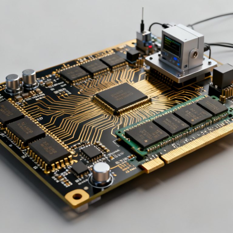
As data centers evolve to support 400G and 800G Ethernet standards, the demand for high-speed optical modules has skyrocketed. These modules—such as QSFP-DD, OSFP, and CFP8—require PCBs that can handle extreme signal integrity, thermal management, and miniaturization. The PCB substrate, whether rigid, flexible, or rigid-flex, is the critical enabler of 400G/800G performance. This Pillar Content page dives deep into the design, material, and manufacturing considerations for high-speed optical module PCBs, drawing from the most authoritative industry sources.
Core Challenges in 400G/800G Optical Module PCB Design
Signal Integrity at 112 Gbps PAM4 for 400G/800G Optical Module PCB
The transition from 25G NRZ to 112 Gbps PAM4 (used in 400G/800G modules) introduces severe signal integrity challenges. At these speeds, even minor impedance mismatches, crosstalk, or dielectric losses can cause bit errors. Key factors include:
- Dielectric Loss (Df): Low Df materials (e.g., <0.002 at 10 GHz) are mandatory to minimize attenuation. Standard FR-4 is inadequate.
- Conductor Surface Roughness: Copper foil with low profile (e.g., RTF or VLP) reduces skin effect losses.
- Impedance Control: Tight tolerance (±5% or better) for differential pairs (e.g., 100Ω for high-speed signals).
- Via Stub Management: Backdrilling or blind/buried vias eliminate stub resonance at high frequencies.
Thermal Management in High-Density Modules
400G/800G optical modules dissipate significant heat (15–30W per module) due to high-speed DSPs, lasers, and drivers. PCB design must:
- Use Thermal Vias: Arrays of vias under hot components to conduct heat to inner copper planes.
- Employ Metal Core PCBs (MCPCB): For modules with extreme thermal loads, aluminum or copper cores are embedded.
- Optimize Copper Thickness: 2 oz or 3 oz copper in power layers reduces resistive heating.
Miniaturization and Layer Count
To fit the compact form factors (e.g., QSFP-DD is 18.35 mm wide), PCBs require:
- High Layer Count: 12–20 layers are common for 400G modules; 800G may need 20+ layers.
- Microvias (HDI): Laser-drilled microvias (≤100 μm) enable dense routing without increasing board size.
- Stack-up Optimization: Symmetric stack-ups with low-Dk prepregs minimize skew and impedance variation.
Material Selection for High-Speed Optical PCBs
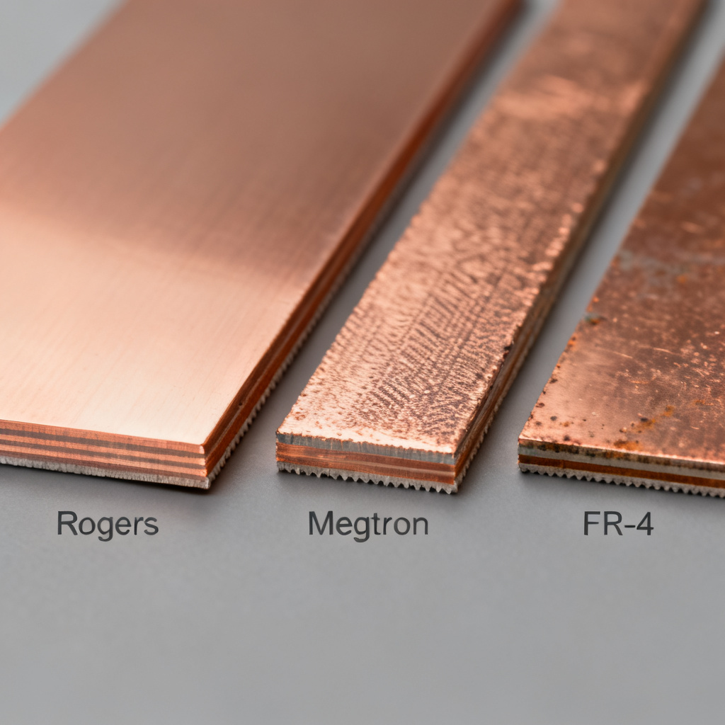
High-Frequency Laminates for 400G/800G Optical Module PCB
The choice of laminate directly impacts signal integrity. Industry-standard materials include:
- Rogers 3003/4350B: Low Df (0.0013–0.0037) and stable Dk (3.0–3.5) across frequency. Used for high-speed differential pairs.
- Isola I-Tera MT40: Low Df (0.0025 at 10 GHz) and high thermal reliability (Tg > 200°C). Suitable for multilayer designs.
- Panasonic Megtron 6/7: Ultra-low Df (0.001–0.002) and low z-axis expansion. Preferred for 800G modules.
- Taconic RF-35: Cost-effective alternative with Df 0.0018, good for receiver/transmitter circuits.
Copper Foil Types
- Reverse Treated Foil (RTF): Reduces insertion loss by 10–15% vs. standard ED foil.
- Very Low Profile (VLP) Foil: Essential for 112 Gbps PAM4 signals; minimizes conductor loss.
- Rolled Annealed (RA) Foil: For flexible circuits (flex PCBs) to withstand bending.
Prepreg and Bonding Materials
- Low-Flow Prepreg: Prevents resin bleed into via holes during lamination.
- High-Tg FR-4 (e.g., IT-180A): Used for non-critical layers (power, ground) to reduce cost.
- Thermally Conductive Prepreg: e.g., T-preg with 2.0 W/mK for heat spreading.
Design Techniques for 400G/800G Optical Module PCBs
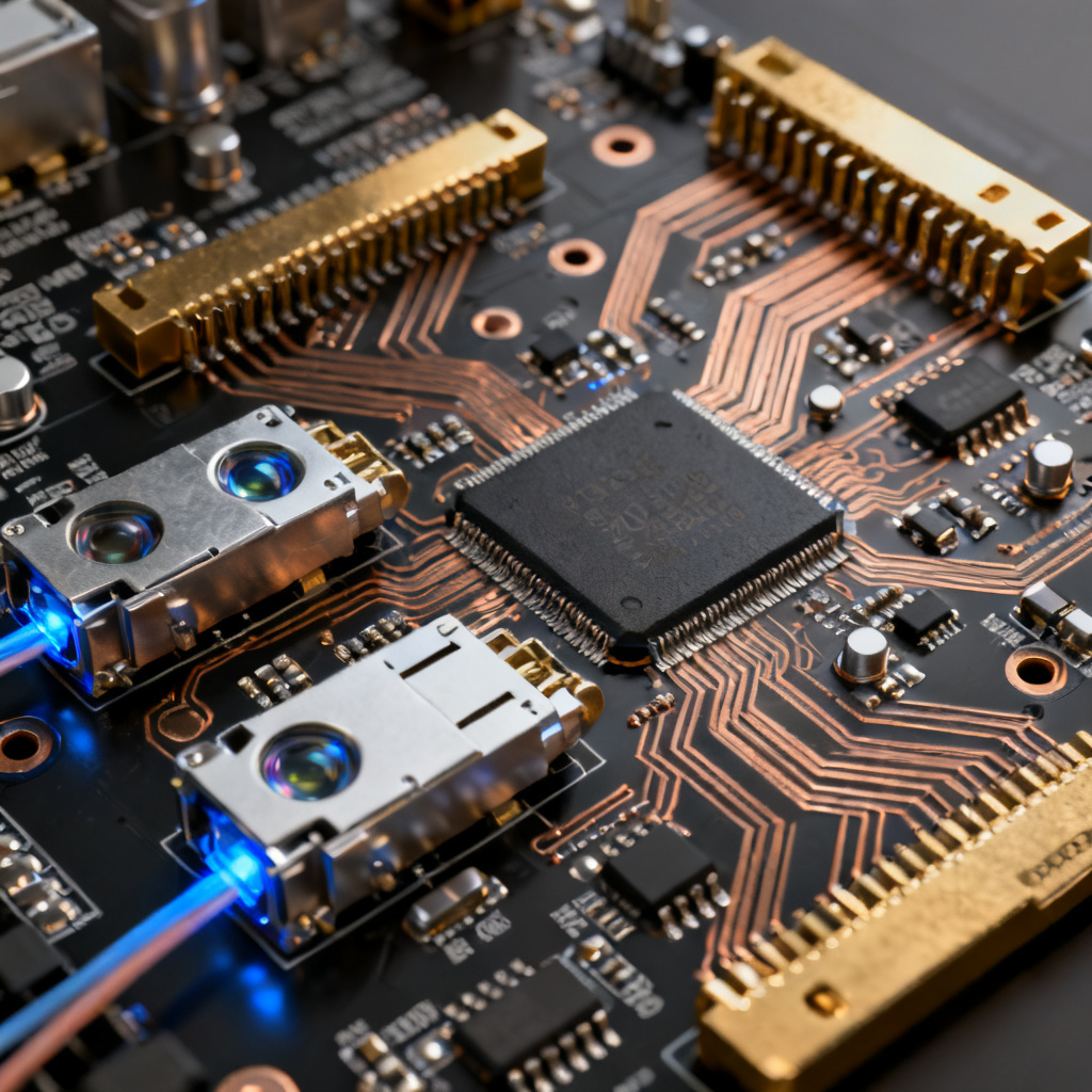
Routing and Impedance Control
For optimal 400G/800G Optical Module PCB performance, routing and impedance control are critical.
- Differential Pair Routing: Keep pair length matching within ±0.1 mm; use serpentine delays for phase alignment.
- Ground Plane Integrity: No splits under high-speed traces; add stitching vias every λ/10 (e.g., 1.5 mm at 112 GHz).
- Avoid 90° Corners: Use 45° chamfered corners or circular arcs to reduce reflections.
Via Design and Backdrilling
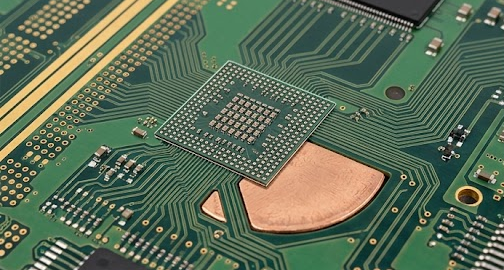
- Via Stub Elimination: Backdrill all vias to within 10 mils of the signal layer. For 800G, use only blind/buried vias.
- Via-in-Pad (VIP): Filled and capped vias under BGA pads improve routing density and thermal performance.
- Via Diameter: 0.2 mm (8 mil) for signal vias; 0.3 mm (12 mil) for thermal vias.
Power Integrity and Decoupling
- Power Distribution Network (PDN): Use wide copper planes (e.g., 2 oz) and multiple vias to reduce inductance.
- Decoupling Capacitors: Place 0.1 μF and 0.01 μF capacitors within 1 mm of DSP/ASIC pins.
- Bulk Capacitors: 10–100 μF tantalum or ceramic capacitors on module edges.
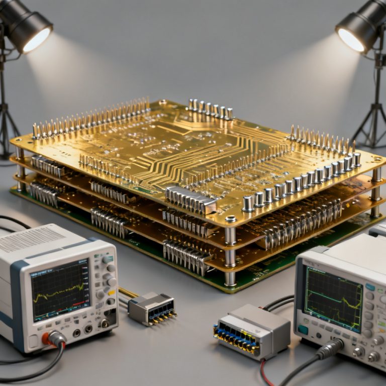
Flex and Rigid-Flex Considerations
For modules requiring dynamic bending (e.g., in server backplanes or cable assemblies):
- Flex Material: Polyimide (Kapton) with 1 oz or 0.5 oz RA copper. Minimum bend radius: 10× thickness.
- Coverlay vs. Solder Mask: Coverlay (polyimide film) is preferred for flex areas to prevent cracking.
- Rigid-Flex Transition Zones: Use teardrop pads and avoid sharp corners to reduce stress.
- Stiffeners: Add FR-4 or polyimide stiffeners in connector areas to maintain flatness.
Manufacturing Process and Quality Control
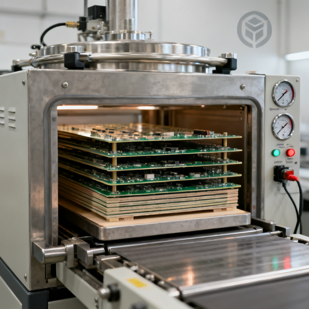
Lamination and Pressing
- Vacuum Lamination: Essential to eliminate voids in high-layer-count boards.
- Pressure Profile: Gradual ramping to 300–400 psi for 90 minutes to ensure resin flow.
- Post-Lamination Cure: 4–8 hours at 150°C to stabilize Dk/Df.
Drilling and Plating
- Laser Drilling: For microvias (≤0.1 mm); UV or CO2 lasers for polyimide.
- Mechanical Drilling: For through-holes; use carbide bits with 150,000+ RPM.
- Plating Uniformity: Electroless copper followed by electrolytic plating; target 25 μm minimum in holes.
Solder Mask and Surface Finish
- Solder Mask: LPI or dry film; color options (green, black) but black absorbs heat.
- Surface Finish: ENIG (0.1–0.3 μm Au) for flat pads; HASL for cost-sensitive designs; OSP for fine-pitch.
- Edge Plating: For grounding EMI shields or connectors.
Electrical Testing and Inspection
- TDR (Time Domain Reflectometry): Verify impedance (e.g., 100Ω ± 5Ω) at 35 ps rise time.
- Insertion Loss Testing: Use VNA (Vector Network Analyzer) up to 50 GHz; target <0.5 dB/inch at 28 GHz.
- Automated Optical Inspection (AOI): Detect shorts, opens, and misregistration.
- X-Ray Inspection: For hidden vias and BGA solder joints.

Applications and Market Trends
400G/800G Optical Module Form Factors
- QSFP-DD (Quad Small Form Factor Pluggable Double Density): 8 electrical lanes; 400G/800G; PCB stack-up typically 16–20 layers.
- OSFP (Octal Small Form Factor Pluggable): 8 lanes; wider than QSFP-DD; requires thermal management with heatsinks.
- CFP8 (C Form-Factor Pluggable 8): 16 lanes; used in early 400G deployments; now less common.
Key End-Use Sectors
- Hyperscale Data Centers: Google, Amazon, Microsoft use 400G/800G for spine-leaf architectures.
- Telecom 5G xHaul: CPRI/eCPRI interfaces require 25G/100G optical links.
- High-Performance Computing (HPC): InfiniBand NDR 400G for GPU clusters.
- Aerospace & Defense: Ruggedized optical modules for radar and satellite comms.
Emerging Trends
- Co-Packaged Optics (CPO): PCBs integrate optical engines directly; requires ultra-low-loss materials.
- Silicon Photonics: PCB substrates must support hybrid integration of SiPh chips.
- 800G on 112 Gbps PAM4: Requires 8 lanes; PCB loss budget <3 dB per link.
Design Guidelines for Engineers
Stack-Up Recommendations
| Stack-Up Type | Layers | Materials |
|---|---|---|
| Low-Cost 400G | 4 layers | Megtron 6 |
| High-Performance 400G/800G | 8 layers | Rogers 4350B + Megtron 6 hybrid |
| Flex-Rigid | 2 flex + 4 rigid | Polyimide + FR-4 or high-speed |
Layout Rules
- Trace Width/Spacing: For 100Ω differential, 0.1 mm width with 0.15 mm spacing (microstrip) or 0.08 mm with 0.1 mm spacing (stripline).
- Keep-Out Zones: 0.5 mm from board edge; 0.3 mm from mounting holes.
- Thermal Relief: For power pads, use 4-spoke thermal relief with 0.2 mm spoke width.
Simulation and Validation
- Use 3D EM Solvers: ANSYS HFSS or CST for full-wave simulation of vias and connectors.
- Eye Diagram Analysis: Ensure >60% eye opening at 112 Gbps.
- Thermal Simulation: FloTherm or Icepak to predict junction temperatures.
Supplier and Certification Considerations
PCB Fabrication Capabilities
| Parameter | Specification |
|---|---|
| Minimum Trace Width | 0.05 mm (2 mil) for HDI; 0.075 mm (3 mil) for standard |
| Aspect Ratio | 10:1 (through-holes); 1:1 (microvias) |
| Board Thickness | 0.8 mm (typical for modules); up to 3.2 mm for backplanes |
Certifications
- IPC Class 3: For high-reliability optical modules (e.g., aerospace).
- UL 94 V-0: Flammability rating for all materials.
- RoHS/REACH: Compliance for European market.
- ISO 9001/AS9100: Quality management for PCB manufacturing.
Testing and Validation Services
- Third-Party Labs: e.g., ETL, Intertek for TDR and loss measurements.
- In-House Testing: Use Tektronix DSA8300 or Keysight N5227B for characterization.
Cost Optimization and Lead Times
Material Cost Breakdown
| Material | Cost per sq ft |
|---|---|
| Rogers 4350B | $50–$80 |
| Megtron 6 | $40–$60 |
| High-Tg FR-4 | $10–$20 |
| Flex Polyimide | $30–$50 |
Lead Time Considerations
- Standard Prototypes: 5–7 business days (4-layer).
- Complex Rigid-Flex: 15–20 business days.
- Volume Production: 4–6 weeks for 20-layer boards.
Cost-Saving Tips
- Use Hybrid Stack-Ups: Mix high-speed and standard materials (e.g., Rogers for signal layers, FR-4 for power).
- Panel Utilization: Optimize panel size (e.g., 18″×24″) to reduce waste.
- Design for Manufacturability (DFM): Avoid via-in-pad if possible; use standard via sizes.
Future Outlook: 1.6T and Beyond
The PCB industry is already preparing for 1.6T optical modules (e.g., OSFP-XD). Key trends:
- 224 Gbps PAM4: Requires materials with Df <0.001 and ultra-smooth copper.
- Glass Core PCBs: Lower CTE and better dimensional stability than organic laminates.
- Embedded Components: Resistors and capacitors embedded in PCB layers to reduce footprint.
Conclusion
Designing and manufacturing PCBs for 400G/800G optical modules is a multi-disciplinary challenge requiring expertise in materials, signal integrity, thermal management, and manufacturing. By adopting low-loss laminates, HDI techniques, and rigorous testing protocols, engineers can achieve the performance required for next-generation data centers and telecom networks. For B2B buyers, partnering with a PCB manufacturer that offers IPC Class 3, high-layer count, and flex-rigid capabilities is critical to success.
Frequently Asked Questions about 400G/800G Optical Module PCB
What is a 400G/800G Optical Module PCB?
A 400G/800G Optical Module PCB is a high-speed printed circuit board designed for optical transceivers that support 400G and 800G Ethernet standards, typically using PAM4 modulation and advanced materials like Megtron or Rogers.
Why is material selection critical for 400G/800G Optical Module PCB?
Material selection is critical because low Df and Dk values are required to maintain signal integrity at 112 Gbps PAM4, reducing insertion loss and crosstalk in the 400G/800G Optical Module PCB.
How does thermal management affect 400G/800G Optical Module PCB design?
Thermal management is vital as 400G/800G modules generate 15–30W heat; using thermal vias, MCPCB, and optimized copper thickness ensures reliable operation of the 400G/800G Optical Module PCB.
What are the key differences between 400G and 800G Optical Module PCBs?
800G Optical Module PCBs require higher layer counts (20+), tighter impedance control, and ultra-low-loss materials compared to 400G versions, due to 112 Gbps PAM4 signaling.
Can flex PCBs be used in 400G/800G Optical Module designs?
Yes, flex and rigid-flex PCBs are used in dynamic applications like server backplanes, with polyimide materials and RA copper to withstand bending while maintaining signal integrity.