This comprehensive guide explores Hybrid PCB Stackups: FR4 + RF Material Design Techniques, the definitive approach for engineers balancing high-frequency performance with cost-effective manufacturing in modern electronics.
In high-frequency electronics, the demand for circuits combining digital, analog, and RF functionality on a single board is relentless. A pure RF laminate like Rogers or Teflon offers excellent electrical performance but is expensive and mechanically fragile. A pure FR4 board is cost-effective but suffers from high dielectric loss and inconsistent impedance at high frequencies. The solution? Hybrid PCB stackups—carefully engineered lamination of FR4 and RF-specific materials. This pillar content explores design techniques, material science, and practical considerations for creating high-performance hybrid PCBs that balance cost, signal integrity, and manufacturability.
We have synthesized the most authoritative insights from leading industry resources to provide the definitive guide.
1. Why Hybrid PCB Stackups: The Core Rationale
A Hybrid PCB Stackup is not a compromise; it is an optimization. The fundamental reason for using a hybrid stackup is to isolate high-speed/RF signals from noisy digital layers while maintaining a cost-effective base structure.
The “Best of Both Worlds” Principle
Hybrid PCB Stackups deliver the best of both worlds through precise material placement:
- RF Performance: The top layers (or specific signal layers) use low-loss RF materials (e.g., Rogers 4003C, Rogers 4350B, PTFE/Teflon) to ensure minimal signal attenuation, consistent dielectric constant (Dk), and low dissipation factor (Df) at frequencies above 1 GHz.
- Structural Integrity & Cost: The core or lower layers use standard FR4 (e.g., IT-180A, FR4-TG170) for mechanical strength, thermal management, and cost reduction. FR4 provides the rigid backbone for connectors, mounting holes, and large ground planes.
Source 1 Insight: The primary driver is cost. A full RF board can be 5-10x more expensive than a hybrid. Hybrid stackups allow you to use expensive RF material only where it is absolutely necessary—on the critical signal layers.
Source 2 Insight: The secondary driver is mechanical reliability. RF materials often have a high Coefficient of Thermal Expansion (CTE) and are softer. FR4 provides the stability needed for through-hole components and board-level reliability during assembly and reflow.
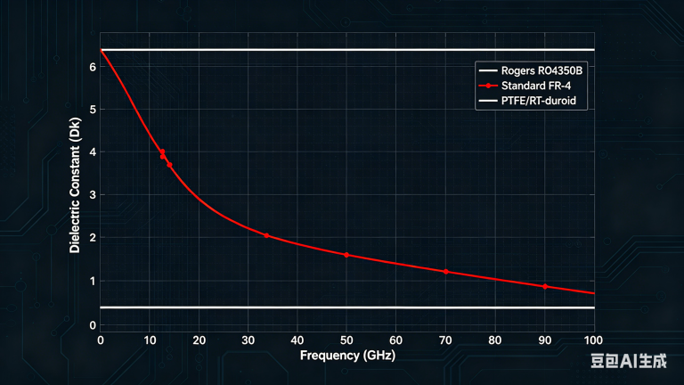
Source 3 Insight: The third driver is impedance control. FR4’s Dk can vary significantly (from 3.8 to 4.8 depending on resin content and frequency). RF materials offer tightly controlled Dk (e.g., 3.48 ± 0.05 for Rogers 4350B), ensuring predictable characteristic impedance for transmission lines (e.g., 50Ω microstrip or stripline).
2. The Material Science Behind Hybrid PCB Stackups
Understanding the materials is critical. A Hybrid PCB Stackup is a multi-layered sandwich where each material serves a specific purpose.
2.1 The RF Laminates (The “High-Performance” Layer)
These are the core of your RF section. The most common choices include:
- Rogers RO4000 Series (RO4003C, RO4350B): Hydrocarbon ceramic laminates offering excellent high-frequency performance (up to 40 GHz), low loss, and stable Dk. Crucially, they are compatible with standard FR4 processing (via etching, drilling, and lamination), making them the most common choice for hybrid PCBs.
- PTFE-based Laminates (Teflon, Rogers RT/duroid): Offer the lowest loss (Df < 0.001) and are used for the most demanding RF applications (e.g., 77 GHz automotive radar, satellite communications). However, they are the most expensive, require specialized plasma treatment for adhesion, and are very difficult to process.
- Other Low-Loss Materials: Isola (e.g., IS620, I-Tera MT40) and Nelco (e.g., N4000-13EP) offer high-performance alternatives that are also FR4-compatible.
Key Parameters to Consider:
- Dielectric Constant (Dk): Must be stable across frequency and temperature. A lower Dk is generally better for high-speed signals.
- Dissipation Factor (Df): The measure of signal loss. Lower is better (e.g., 0.002 for RO4350B vs. 0.02 for standard FR4).
- Coefficient of Thermal Expansion (CTE): Must match FR4 as closely as possible to prevent delamination during thermal cycling.
2.2 The FR4 (The “Structural” Layer)
Standard FR4 is not a single material but a family. For Hybrid PCB Stackups, High-Tg FR4 (e.g., TG170, TG180) is strongly recommended.
- Why High-Tg? RF materials often have higher processing temperatures. High-Tg FR4 (Glass Transition Temperature >170°C) ensures the board does not soften or warp during the multi-lamination cycles required for hybrid boards.
- Why not standard FR4? Standard FR4 (Tg 130-140°C) can exhibit significant dimensional instability and Z-axis expansion during the high-temperature reflow of RF components, leading to via barrel cracking.
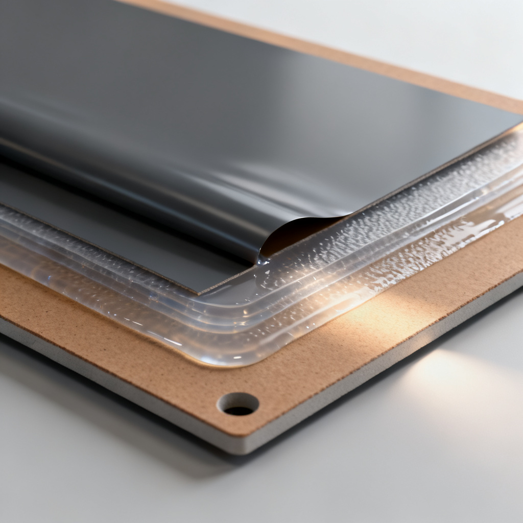
2.3 The Bonding Layer: The Critical Interface
The most technically challenging part of a Hybrid PCB Stackup is bonding the RF material to the FR4. You cannot simply use standard FR4 prepreg.
- The Problem: RF materials (especially PTFE) are chemically inert and non-porous. Standard FR4 prepreg will not bond to them reliably. The bond will fail under thermal stress.
- The Solution: Use a bonding film or specialized prepreg. Common choices include:
- Rogers 2929 Bondply: A high-performance bonding film designed for RO4000 series laminates. It provides excellent adhesion and low loss.
- Panasonic R-5680: A low-flow, low-loss prepreg used for high-speed digital and RF hybrids.
- Thermount (e.g., 1000, 2000): A non-woven aramid fiber prepreg used for bonding PTFE to FR4. It is expensive but provides excellent thermal and mechanical properties.
Source 1 Insight: Never use standard FR4 prepreg to bond an RF core to an FR4 core. This is the most common cause of field failures. Always specify the correct bonding film.
Source 2 Insight: The bonding layer also acts as a dielectric. Its Dk and Df must be considered in your impedance calculations. The overall stackup is a series of dielectrics: RF core + Bonding film + FR4 core + Prepreg.
3. Design Techniques for Successful Hybrid PCB Stackups
This section details the practical steps and rules you must follow during the PCB layout phase for Hybrid PCB Stackups.
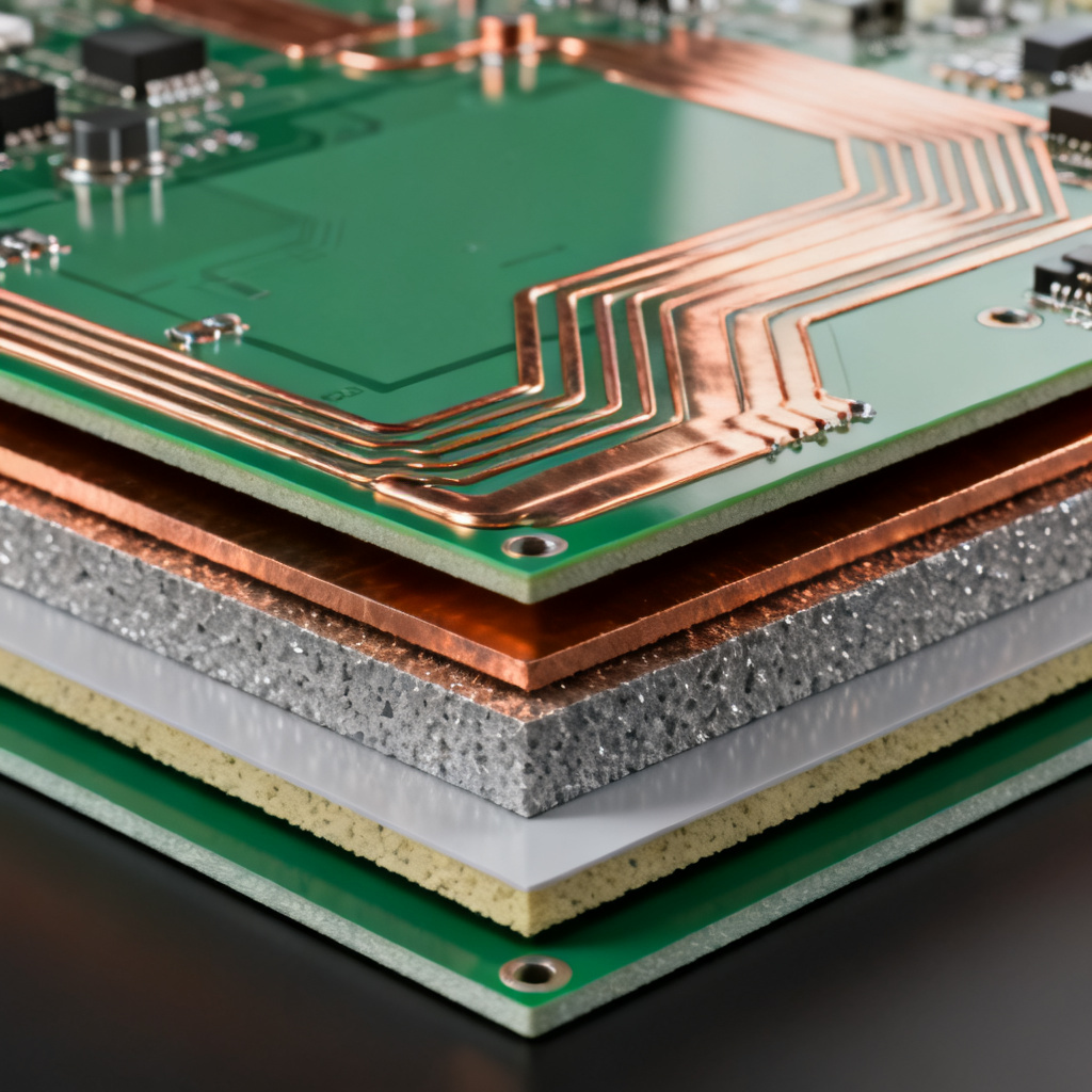
3.1 Stackup Architecture: The “Sandwich” Design
There are two primary architectures for Hybrid PCB Stackups:
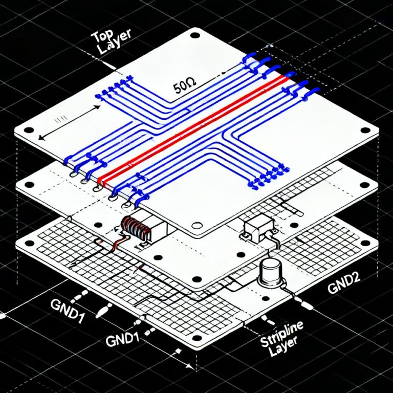
A. The “Cap” or “Top Layer” Hybrid (Most Common)
- Layer 1 (Top): RF Material (e.g., Rogers 4350B) – This is where the RF traces, antennas, and critical high-speed signals are placed.
- Layer 2 (Ground): Solid ground plane (usually copper). This provides a reference for the RF signals and isolates them from the digital layers below.
- Layer 3 (Inner): FR4 Core – Digital signals, power planes, and slower analog signals.
- Layer 4 (Bottom): FR4 – Additional digital signals or a bottom ground plane.
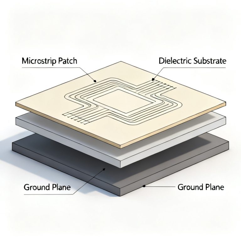
B. The “Core” or “Embedded” Hybrid
- Layer 1 (Top): FR4 – Digital signals.
- Layer 2 (Ground): Solid ground plane.
- Layer 3 (Inner – RF Core): RF Material – Dedicated for high-frequency stripline routing.
- Layer 4 (Bottom): FR4 – Additional signals or ground.
Source 3 Insight: Always place the RF material adjacent to a solid ground plane. This minimizes crosstalk and provides a clean return path for RF currents. Never embed an RF signal layer between two digital signal layers.
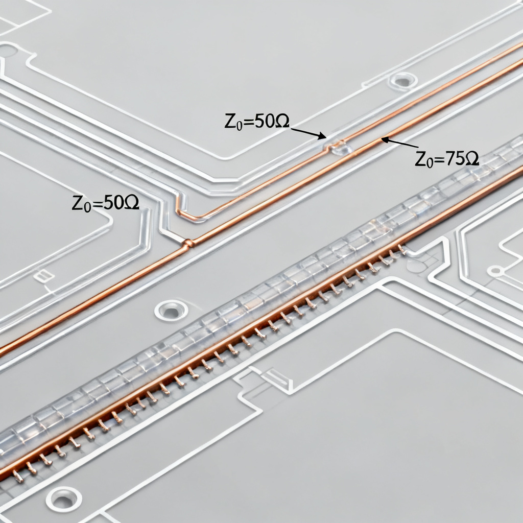
3.2 Impedance Control & Trace Design for Hybrid PCB Stackups
This is where the hybrid nature becomes critical.
- Trace Width Calculation: You must calculate the trace width for 50Ω (or other target impedance) using the Dk of the RF material for the top layer and the bonding film + FR4 for embedded layers. Do not use a single Dk value.
- Microstrip vs. Stripline: Microstrip (top layer) is easier to fabricate and offers lower loss. Stripline (embedded in RF core) offers better isolation and is preferred for very sensitive RF paths.
- Copper Roughness: RF materials often use smooth copper (e.g., RTF or VLP copper) to minimize skin effect losses at high frequencies. If your RF traces are on the outer layer, specify smooth copper for that layer. The inner layers of FR4 can use standard ED copper.
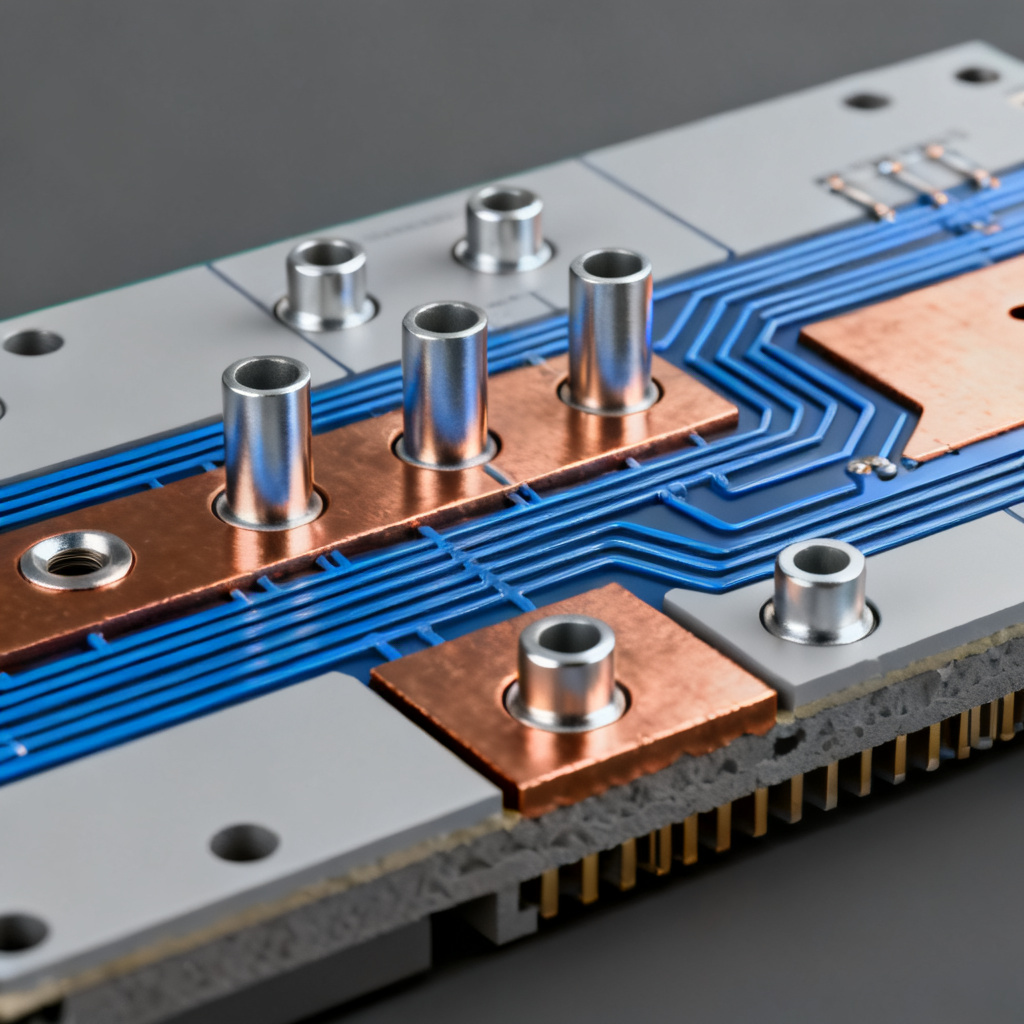
3.3 Via Management in Hybrid PCB Stackups
Vias are a major source of signal degradation in hybrid boards.
- Via Stubs: A via that passes through the entire board creates a stub that resonates at certain frequencies. Use back-drilling to remove the stub length from the RF signal layer to the adjacent ground plane.
- Via Tenting: Use tented vias (covered with solder mask) on the RF layers to prevent solder wicking and impedance changes during assembly.
- Via-in-Pad: Avoid placing vias directly in RF pads if possible. If unavoidable, fill them with conductive epoxy (e.g., ViaPlug) and planarize them.
Source 1 Insight: Back-drilling is mandatory for any hybrid stackup operating above 5 GHz. Without it, the via stub will act as a quarter-wave resonator, causing significant insertion loss.
Source 2 Insight: For vias that transition from the RF layer to the FR4 layers, the impedance discontinuity is less of a concern if the via diameter is small (< 0.3mm) and the ground plane is close.
3.4 Thermal Management for Hybrid PCB Stackups
RF components (power amplifiers, LNAs) generate heat. FR4 is a poor thermal conductor.
- Thermal Vias: Place an array of small, filled thermal vias under hot RF components to conduct heat down to the FR4 core, which can then spread it.
- Copper Coin or Inlay: For very high-power applications, consider a copper coin or inlay embedded in the FR4 layer directly under the RF component. This provides a low-thermal-resistance path to the board’s backside.
- Metal Core PCB (MCPCB) Integration: In extreme cases, the hybrid stackup can be bonded to an aluminum or copper baseplate for active cooling.
4. Manufacturing & Fabrication Challenges for Hybrid PCB Stackups
Designing a hybrid board is only half the battle. You must work closely with a manufacturer who has experience with these materials and Hybrid PCB Stackups.
4.1 Lamination Process
- Temperature & Pressure Profile: The lamination cycle for a hybrid board is different from a standard FR4 board. The bonding film requires a specific temperature and pressure profile to cure correctly without damaging the RF material.
- Multi-Step Lamination: Some hybrid stackups require a two-step lamination process. First, the RF core is laminated to its prepreg. Then, the entire assembly is laminated to the FR4 core. This adds cost and lead time.
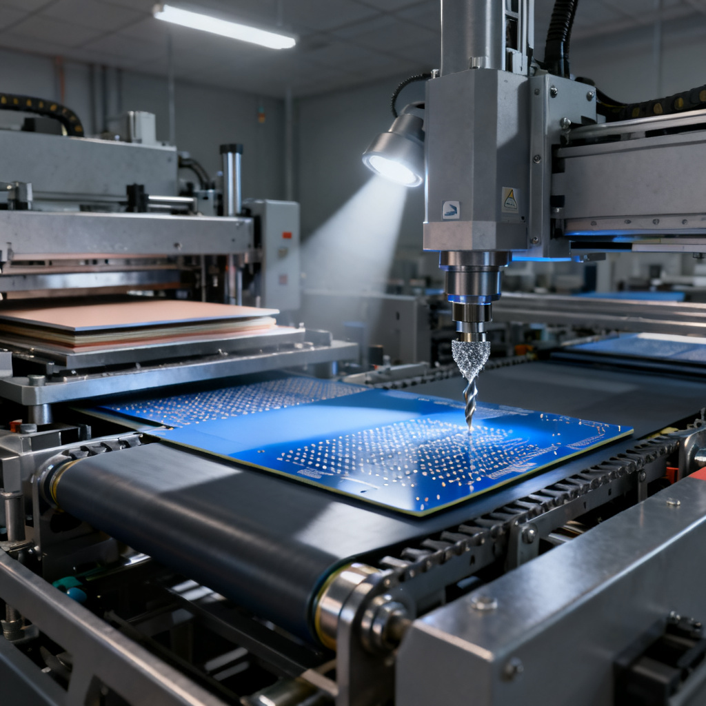
4.2 Drilling & Plating
- Drill Bit Wear: RF materials (especially PTFE and ceramic-filled hydrocarbons) are abrasive and will dull drill bits faster than FR4. This can lead to rough hole walls and poor plating adhesion.
- Desmear: Standard FR4 desmear (plasma or permanganate) may not be sufficient for RF materials. A more aggressive plasma desmear is often required to ensure good copper plating adhesion inside the via hole.
4.3 Surface Finish
- ENIG (Electroless Nickel Immersion Gold): The industry standard for RF boards. It provides a flat, solderable surface with good corrosion resistance. Ensure the nickel thickness is tightly controlled to avoid magnetic interference.
- Immersion Silver (ImAg): A cheaper alternative, but can tarnish. Not recommended for very high-frequency (>20 GHz) applications.
- HASL (Hot Air Solder Leveling): Avoid HASL. The uneven surface and thermal shock can damage the RF material and create impedance discontinuities.
Source 3 Insight: Always request a “Cross-Section” report from your fabricator. This will verify the actual thickness of each layer (RF core, bonding film, FR4 core, prepreg) and confirm that your impedance calculations are accurate.
5. Step-by-Step Design Checklist for Hybrid PCB Stackups
To ensure success, follow this checklist before sending your design to fabrication:
- Define RF Requirements: What is the maximum frequency? What is the target impedance (e.g., 50Ω, 75Ω, 100Ω differential)?
- Select RF Material: Choose Rogers RO4000 series for most applications. Choose PTFE for >40 GHz or extremely low loss.
- Select FR4 Core: Use High-Tg FR4 (TG170+).
- Select Bonding Film: Use Rogers 2929 for RO4000 series. Use Thermount for PTFE.
- Design Stackup: Place RF material on outer layer(s) adjacent to a solid ground. Use a “Cap” or “Core” architecture.
- Calculate Impedance: Use the Dk of the RF material and the bonding film separately. Do not average them.
- Specify Copper: Use smooth copper (RTF/VLP) on RF layers.
- Manage Vias: Use back-drilling for all RF vias. Fill vias under RF pads.
- Add Thermal Management: Use thermal vias or copper coins for power components.
- Choose Surface Finish: Use ENIG. Avoid HASL.
- Select a Qualified Manufacturer: Ask for references for hybrid PCBs. Require cross-section reports.
- Review DFM (Design for Manufacturing): Ensure your board house can handle the required lamination cycles and drill bit changes.
Key Parameters Comparison Table for Hybrid PCB Stackups
| Parameter | RF Material (e.g., Rogers 4350B) | FR4 (Standard) | High-Tg FR4 (TG170+) |
|---|---|---|---|
| Dielectric Constant (Dk) @ 10 GHz | 3.48 ± 0.05 | 3.8–4.8 (variable) | 3.8–4.5 (variable) |
| Dissipation Factor (Df) | 0.0037 | 0.02 | 0.015 |
| CTE (Z-axis, ppm/°C) | 35–40 | 50–70 | 40–50 |
| Tg (°C) | >280 (decomposition) | 130–140 | >170 |
| Relative Cost | High | Low | Medium |
Frequently Asked Questions (FAQ) about Hybrid PCB Stackups
What is a Hybrid PCB Stackup?
A Hybrid PCB Stackup is a multi-layer printed circuit board that combines different dielectric materials—typically FR4 for cost-effective structural layers and an RF-grade material like Rogers or PTFE for high-frequency signal layers—to optimize both performance and cost.
Why choose FR4 + RF material over a single material?
Choosing Hybrid PCB Stackups allows you to use expensive, high-performance RF material only where needed for signal integrity, while the rest of the board uses cost-effective FR4. This approach significantly reduces overall material costs without compromising high-frequency performance.
How do I calculate impedance for a hybrid stackup?
For accurate impedance control in Hybrid PCB Stackups, you must calculate trace width using the Dk of the RF material for top-layer traces and the combined Dk of the bonding film and FR4 for embedded traces. Do not use a single average Dk value.
What is the best bonding film for hybrid PCBs?
The best bonding film depends on your RF material. For Rogers RO4000 series, Rogers 2929 Bondply is recommended. For PTFE-based materials, Thermount is the standard choice. Never use standard FR4 prepreg as a bonding layer in Hybrid PCB Stackups.
Is back-drilling necessary for hybrid PCBs?
Yes, back-drilling is mandatory for any Hybrid PCB Stackup operating above 5 GHz. It removes via stubs that can cause resonant losses and signal degradation.
Conclusion: Why Your Business Needs Hybrid PCB Stackup Expertise
Hybrid PCB Stackups are the most efficient way to build modern, multi-function electronic systems. They allow you to integrate high-performance RF circuits with cost-effective digital logic on a single board, reducing size, weight, and assembly costs. However, they are not a “set it and forget it” technology. They demand a deep understanding of material science, precise impedance control, and close collaboration with an experienced fabricator. By mastering the techniques outlined in this guide, you can design hybrid PCBs that perform reliably, stay within budget, and meet the most demanding specifications.
Ready to build your next high-frequency design? Contact our engineering team today to discuss your hybrid stackup requirements. We specialize in complex multi-layer laminations and can help you choose the perfect material combination for your application.