Master antenna PCB design for microstrip and phased array systems. Learn substrate selection, impedance control, loss tangent management, thermal considerations, and manufacturing best practices for high-reliability RF PCBs.
Microstrip Antenna PCB Design: Core Principles
What is a Microstrip Antenna?
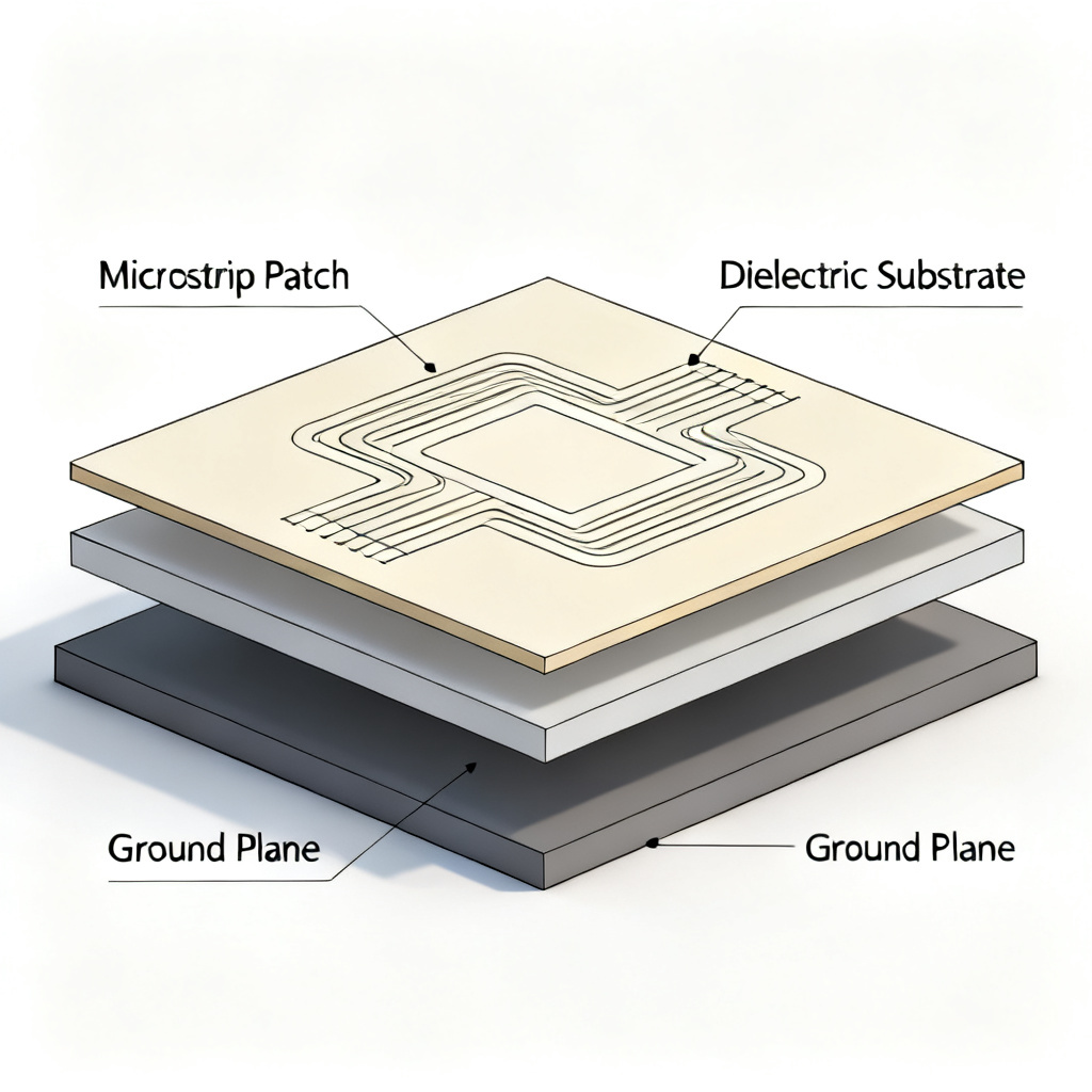
A microstrip antenna consists of a metallic patch (radiating element) on one side of a dielectric substrate, with a ground plane on the opposite side. It is a planar, low-profile structure ideal for frequencies from 1 GHz to over 100 GHz. The patch shape can be rectangular, circular, or triangular, with rectangular being the most common due to ease of analysis and fabrication. Antenna PCB design for microstrip patches requires careful control of patch length (L), patch width (W), substrate thickness (h), and dielectric constant (εr).
Feeding Techniques
The way you feed energy into the patch directly impacts impedance matching and radiation pattern. Three primary methods are:
- Microstrip Line Feed: A conducting strip directly connected to the patch edge. Simple to fabricate but can cause spurious radiation.
- Probe Feed (Coaxial): Inner conductor of a coax passes through the substrate to the patch. Offers easy impedance matching but adds parasitic inductance at high frequencies.
- Aperture Coupling: A slot in the ground plane couples energy from a feed line below. Provides isolation between feed and patch, reducing spurious radiation. Ideal for multilayer designs.
- Proximity Coupling: Two layers of substrate; the feed line is on the bottom, and the patch is on top. No direct contact, offering the broadest bandwidth.
Design Tip: For phased arrays, aperture coupling is often preferred because it eliminates DC connections between active components and radiating elements, simplifying biasing.
Impedance Matching and Bandwidth
Microstrip antennas are inherently narrowband (2–5% fractional bandwidth). To improve bandwidth in antenna PCB design: increase substrate thickness (h), use low-εr materials (e.g., 2.2 to 3.5), or employ stacked patches. Standard 50-ohm matching is achieved through careful simulation of the feed point.
Radiation Pattern and Gain
The radiation pattern of a microstrip patch is broad, with a half-power beamwidth of about 70°–100°. Gain ranges from 4–7 dBi for a single element. To increase gain: use an array of patches, add a superstrate, or employ a reflector. Surface waves generated in thick substrates reduce gain, so use substrates with a low loss tangent (tan δ < 0.002).
Phased Array Substrates: Material Science & Stackup
Why Substrate Choice Matters in Phased Arrays
Phased array antennas rely on precise phase control across hundreds or thousands of elements. Any variation in dielectric constant (εr) across a panel or over temperature will cause phase errors, degrading beam steering accuracy. Therefore, substrate selection is the most critical decision in antenna PCB design for phased arrays.
Key Requirements for Phased Array Substrates:
- Tight εr Tolerance: ±0.05 or better.
- Low Loss Tangent (tan δ): < 0.002 at 10 GHz.
- Thermal Stability: CTE matches copper.
- Consistency Across Panels.
Recommended Material Families
Based on industry standards, the following materials are widely used:
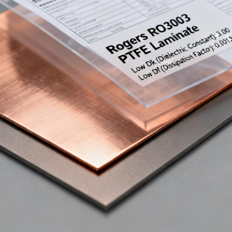
- PTFE/Woven Glass (e.g., Rogers RO4000 series, Taconic RF-35): Low loss, stable εr, good thermal conductivity.
- Hydrocarbon/Ceramic (e.g., Rogers RO3003, Isola Astra MT77): Very low loss (tan δ < 0.0013) and excellent phase stability.
- LCP (Liquid Crystal Polymer): Flexible, low moisture absorption, low loss.
- High-Tg FR-4 Variants: Only for low-frequency (< 2 GHz) or cost-sensitive designs.
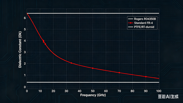
Avoid: Standard FR-4, CEM-1, or any material with high moisture absorption.
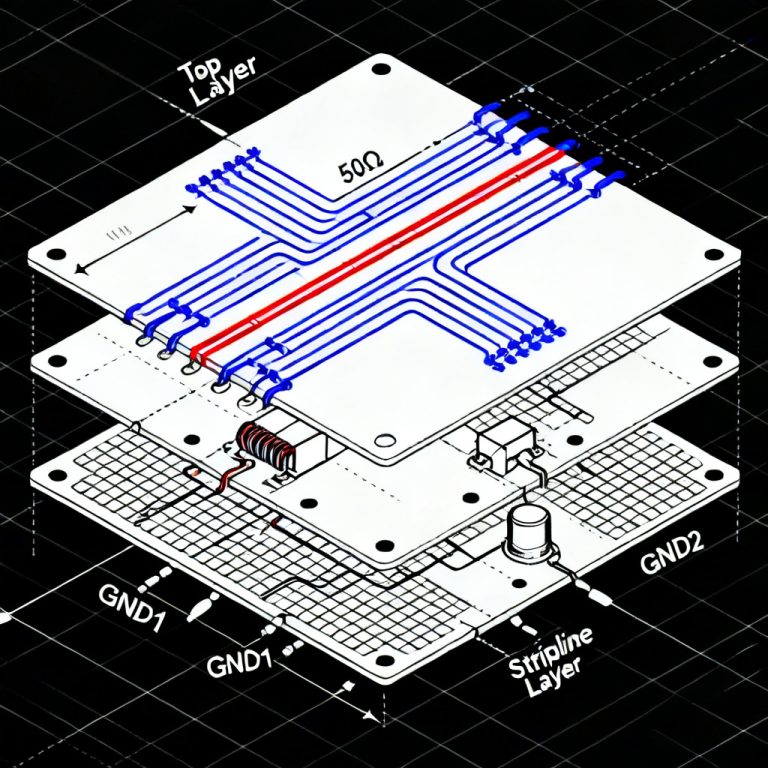
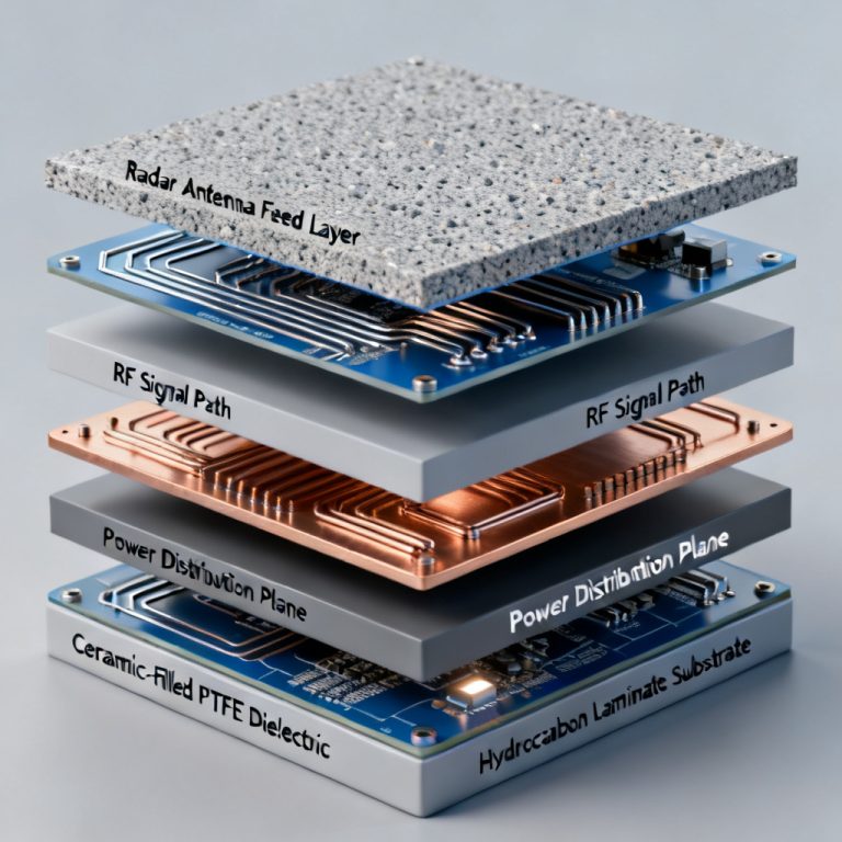
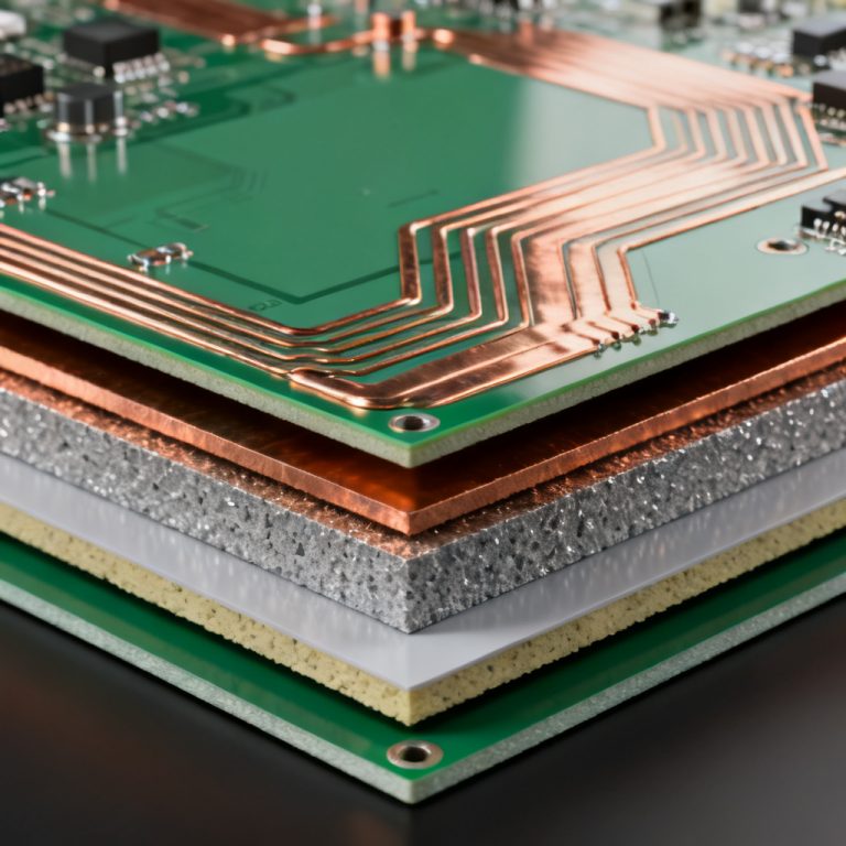
Stackup Design for Phased Arrays
A typical phased array PCB has multiple layers: signal, ground, and power. The stackup must be symmetric to prevent warpage.
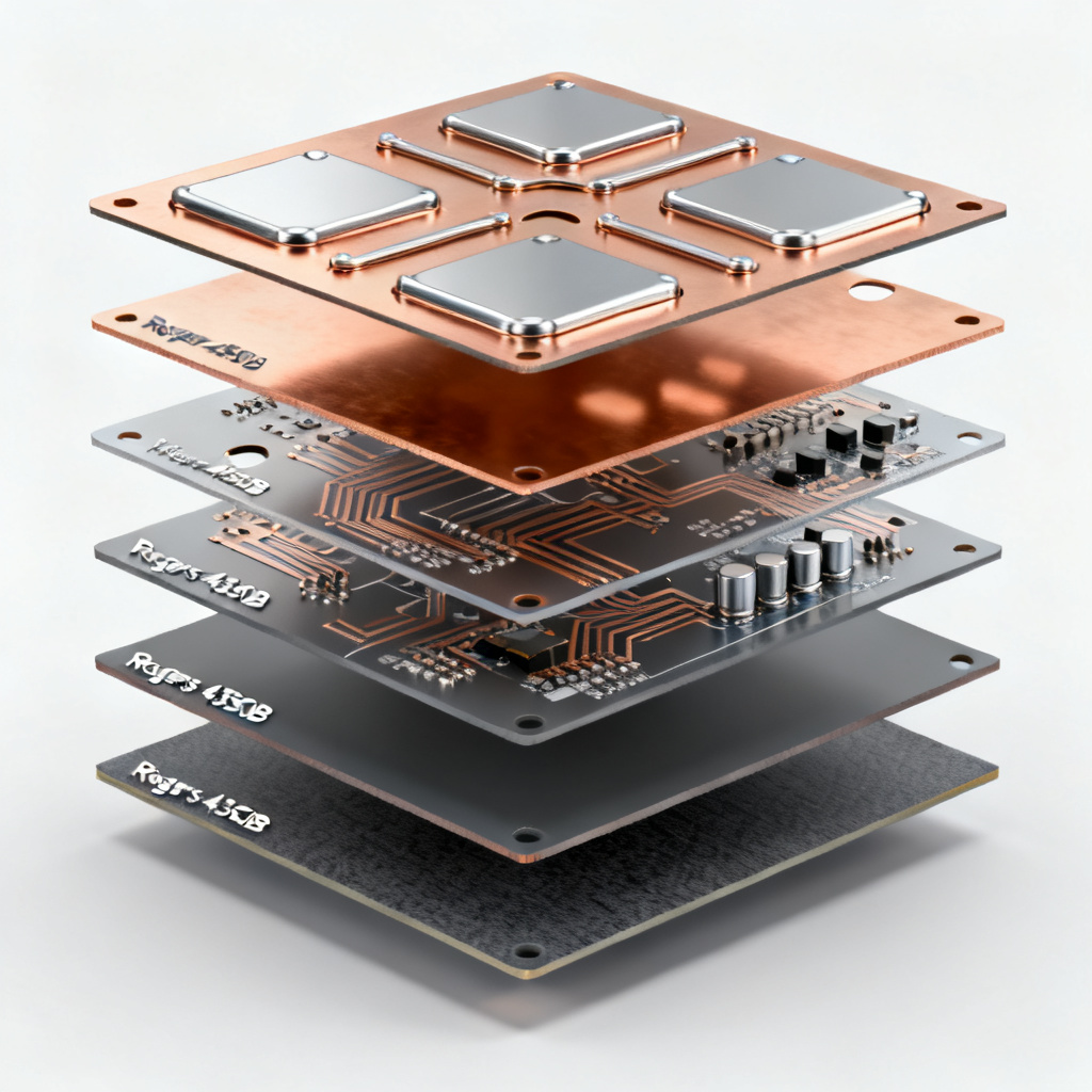
Example 6-Layer Stackup for 28 GHz Phased Array:
| Layer | Function | Material & Thickness |
|---|---|---|
| Layer 1 (Top) | Antenna patches | Rogers RO4350B, 10 mils |
| Layer 2 | Ground plane | Solid copper |
| Layer 3 | Feed network | RO4350B, 20 mils |
| Layer 4 | Ground plane | Solid copper |
| Layer 5 | DC/Bias | FR-4 (isolated from RF) |
| Layer 6 (Bottom) | Ground/control | Solid copper |
Critical Design Rule: Keep the distance between the antenna layer and its ground plane as thin as possible (5–10 mils) to suppress surface waves.
Thermal Management in Phased Arrays
Phased arrays generate significant heat due to multiple power amplifiers and beamformer ICs. Key strategies: use thermally conductive dielectrics like Rogers 4350B (0.62 W/m·K), add thermal vias, consider metal core PCBs (MCPCB), or embed copper coins for localized hot spots.
Design for Manufacturing (DFM) & Testing

Manufacturing Tolerances
High-frequency antenna PCB design requires tighter tolerances: etching tolerance ±0.5 mil, dielectric thickness tolerance ±1 mil, registration ±2 mils, via positioning ±1 mil. Request controlled impedance testing (TDR) for every production panel.
Surface Finish Selection
- ENIG: Good for solderability, but nickel adds loss at high frequencies.
- Immersion Silver: Lower loss, good for wire bonding.
- OSP: Lowest cost, poor shelf life.
- Hard Gold: For edge connectors.
For millimeter-wave (> 30 GHz): Immersion silver or direct gold plating is preferred.
Testing and Validation
- Vector Network Analyzer (VNA) Measurements: S11, S21, phase matching.
- Antenna Pattern Measurement in anechoic chamber.
- Thermal Cycling: -40°C to +85°C for 100 cycles.
- Impedance Profile (TDR).
Production Testing: Every panel should undergo automated RF testing.
Advanced Techniques for High-Performance Antenna PCBs
Artificial Magnetic Conductors (AMC) and EBG Structures
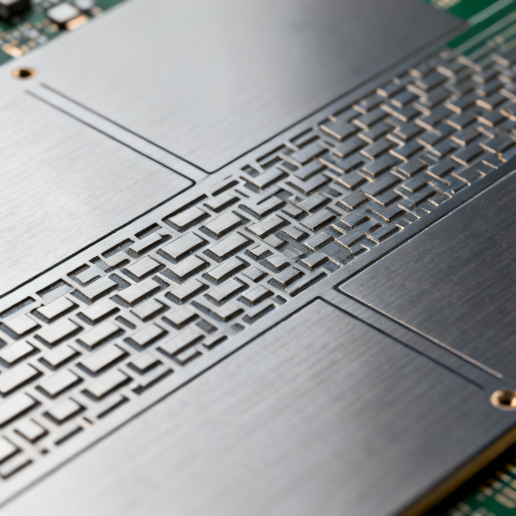
To reduce mutual coupling between array elements, incorporate Electromagnetic Bandgap (EBG) structures or AMC surfaces. These suppress surface waves and improve isolation by 10–20 dB. EBG cells should be sized at λ/4 at the operating frequency.
Dual-Polarized and Circularly Polarized Designs
- Dual-Polarized: Use a square patch with two orthogonal feed points.
- Circular Polarization: Achieved by truncating corners of a square patch or using a 90° hybrid coupler.
Beamforming Network Integration
Phased arrays require a beamforming network (BFN) implemented as a Butler Matrix, corporate feed network, or digital beamforming. Keep digital and RF traces separated by at least 3x the dielectric thickness.
3D Printed and Additive Manufacturing Integration
Emerging techniques allow printing of antenna structures directly on 3D substrates or conformal surfaces, creating dielectric lenses or radomes that improve gain.
Common Pitfalls and How to Avoid Them
| Pitfall | Consequence | Solution |
|---|---|---|
| Using FR-4 for > 2 GHz | High loss, pattern distortion | Switch to Rogers or Taconic |
| Ignoring surface waves | Reduced gain, pattern nulls | Keep substrate thickness < 0.02λ₀ |
| Inconsistent εr across panel | Beam steering errors | Specify εr tolerance, use same batch |
| Poor via stitching | Ground bounce, EMI | Add vias every λ/20 around RF edges |
| Insufficient thermal vias | IC overheating | Use 9+ vias per IC pad with 0.3mm drill |
| Not simulating mutual coupling | Scan blindness in arrays | Simulate with full-wave solver, add EBG |
Partnering with a High-Quality PCB Manufacturer
For antenna PCB design, your manufacturer must demonstrate material traceability, controlled impedance capability, laser direct imaging (LDI), multilayer registration of ±1 mil, and RF testing facility access.
Questions to Ask Your Manufacturer:
- Can you source Rogers RO4350B with a εr tolerance of ±0.05?
- What is your typical etching yield for 4 mil lines on 10 mil substrate?
- Do you offer thermal cycling testing for each panel?
- Can you provide a full RF test report (S-parameters) for phased array panels?
Frequently Asked Questions (FAQ)

What is the best substrate for antenna PCB design in phased arrays?
The best substrate for antenna PCB design in phased arrays is a low-loss material like Rogers RO4350B or RO3003, offering tight εr tolerance and low loss tangent.
How do I improve bandwidth in microstrip antenna PCB design?
To improve bandwidth in antenna PCB design, increase substrate thickness, use low-εr materials, or employ stacked patches.
What is the role of thermal management in phased array antenna PCB design?
Thermal management in phased array antenna PCB design is critical to prevent overheating of power amplifiers and beamformer ICs, using thermal vias, MCPCB, or copper coins.
Can I use FR-4 for antenna PCB design above 2 GHz?
No, FR-4 is not recommended for antenna PCB design above 2 GHz due to high loss and inconsistent dielectric constant.
Conclusion: Building for the Future
Antenna PCB design for microstrip and phased array systems demands precision at every stage—from material selection to manufacturing. By leveraging the insights from this pillar page, you can avoid costly redesigns, achieve first-pass success, and deliver high-performance antennas that meet the rigorous demands of 5G, radar, and satellite communications.
“`