High-frequency microwave PCBs are no longer passive interconnects—they are active RF components that define system performance at mmWave frequencies. This high-frequency microwave PCBs design guide provides a complete engineering framework covering material selection, stackup architecture, impedance control, via engineering, and manufacturing considerations for RF and millimeter-wave applications up to 86 GHz and beyond. Whether you are developing 5G front-ends, automotive radar, or satellite communication systems, the following guidelines establish the foundation for predictable, reliable high-frequency microwave PCBs that meet stringent insertion loss and phase stability requirements.
Design Requirements for High-Frequency Microwave PCBs
High-frequency microwave PCBs demand clearly defined requirements before any layout work begins. High-frequency microwave PCBs operating at mmWave frequencies require documentation of operating frequency range, signal power levels, target impedance (typically 50Ω single-ended), component placement constraints, board dimensions, and environmental conditions. High-frequency microwave PCBs without a documented requirements baseline risk performance deviations that compromise link budgets and phase stability.
Defining Operating Parameters for High-Frequency Microwave PCBs
The wavelength-dependent design rules for high-frequency microwave PCBs are determined by the maximum operating frequency. At 28 GHz, the quarter-wavelength in typical laminates measures approximately 1.3 mm, making trace length control critical. High-frequency microwave PCBs intended for power amplifier applications must additionally specify thermal dissipation targets and peak power handling requirements.
Documenting Impedance Targets for High-Frequency Microwave PCBs
Controlled impedance is non-negotiable in high-frequency microwave PCBs. The design requirements document must explicitly state single-ended impedance (typically 50Ω) and any differential pair targets. High-frequency microwave PCBs fabricated without documented impedance targets often exhibit excessive return loss, degrading overall system performance.
Material Selection for High-Frequency Microwave PCBs
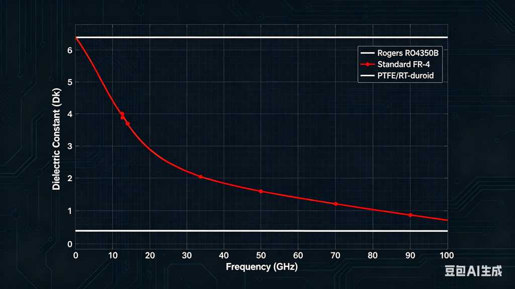
High-frequency microwave PCBs require substrate materials with stable dielectric constant (Dk), low dissipation factor (Df), and controlled thermal expansion. High-frequency microwave PCBs operating above 24 GHz are particularly sensitive to dielectric losses and copper surface roughness, making material selection the single most consequential decision in the design flow.
Key Material Parameters for High-Frequency Microwave PCBs
| Parameter | Definition | Importance for High-Frequency Microwave PCBs |
|---|---|---|
| Dk (Dielectric Constant) | Ratio of material permittivity to vacuum permittivity | Determines wavelength and trace width for controlled-impedance high-frequency microwave PCBs |
| Df (Dissipation Factor) | Measure of dielectric loss tangent | Directly impacts insertion loss in high-frequency microwave PCBs |
| TCDk (Temperature Coefficient of Dk) | Dk variation with temperature | Critical for phase-sensitive high-frequency microwave PCBs in phased-array systems |
| CTE (Coefficient of Thermal Expansion) | Dimensional change with temperature | Affects reliability of high-frequency microwave PCBs in multilayer constructions |
| Copper Surface Roughness (RMS) | Peak-to-valley measurement of copper profile | Increases conductor loss in high-frequency microwave PCBs via skin effect at mmWave frequencies |
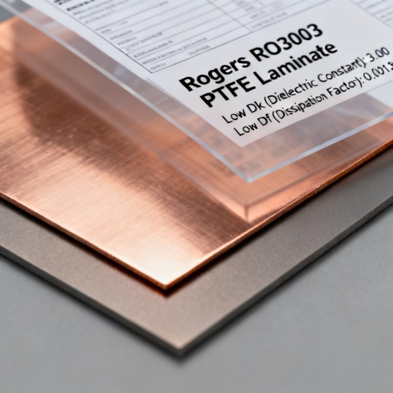
Rogers Materials for High-Frequency Microwave PCBs
High-frequency microwave PCBs frequently utilize Rogers Corporation laminates due to their industry-leading performance. RO4350B (Dk = 3.48 ± 0.05, Df = 0.0037 at 10 GHz) offers FR-4 process compatibility for cost-effective high-frequency microwave PCBs in volume production. For high-frequency microwave PCBs requiring exceptional temperature stability, RO3003 (Dk = 3.00 ± 0.04) and RT/duroid 5880 (Dk = 2.20 ± 0.02) provide ultra-low-loss performance suitable for applications above 40 GHz.
Taconic Materials for High-Frequency Microwave PCBs
High-frequency microwave PCBs can also leverage Taconic laminates where specific performance advantages are required. RF-35 (Dk = 3.5 ± 0.05, Df = 0.0018) offers exceptionally low loss tangent for high-frequency microwave PCBs in ultra-low-loss systems, while TLY-5 and TLX families provide lightweight PTFE compositions with low moisture absorption suitable for aerospace high-frequency microwave PCBs.
Application-Specific Recommendations for High-Frequency Microwave PCBs
| Application | Recommended Material for High-Frequency Microwave PCBs | Key Rationale |
|---|---|---|
| 5G Base Stations | Rogers RO4350B | Superior thermal conductivity (0.71 W/m·K) supports high-power high-frequency microwave PCBs |
| Automotive Radar (77 GHz) | Rogers RO4835 or RO3003 | Temperature stability and oxidation resistance for automotive high-frequency microwave PCBs |
| Satellite Communication | Taconic TLY-5 | Low moisture absorption in space-grade high-frequency microwave PCBs |
| mmWave (>40 GHz) | Rogers RT/duroid 5880 | Ultra-low Dk and Df for precision high-frequency microwave PCBs |
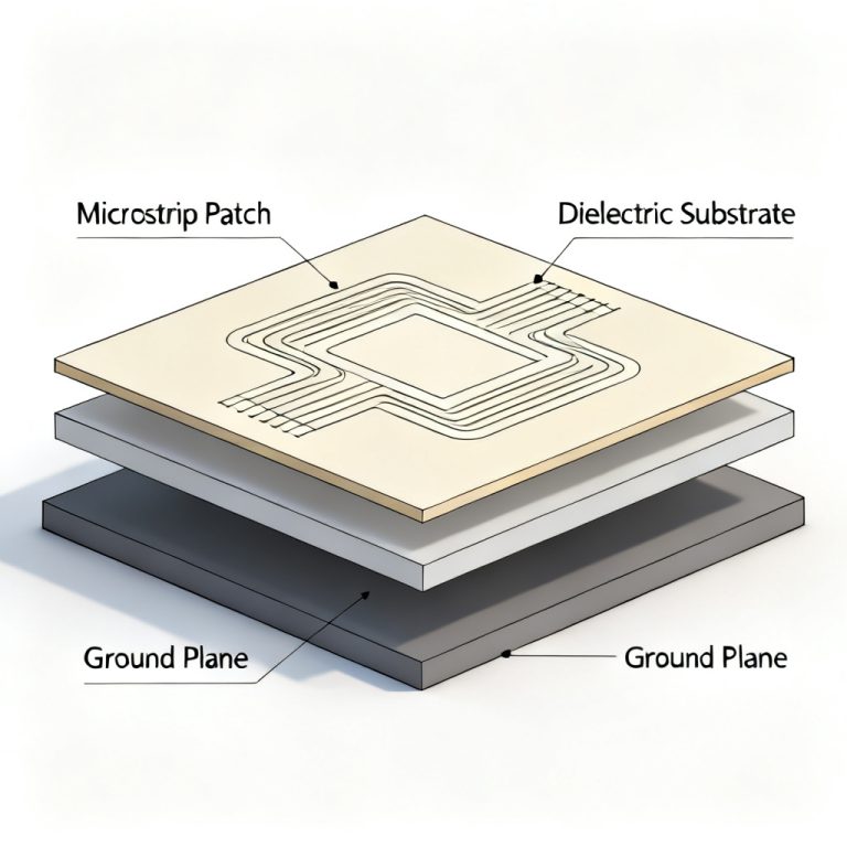
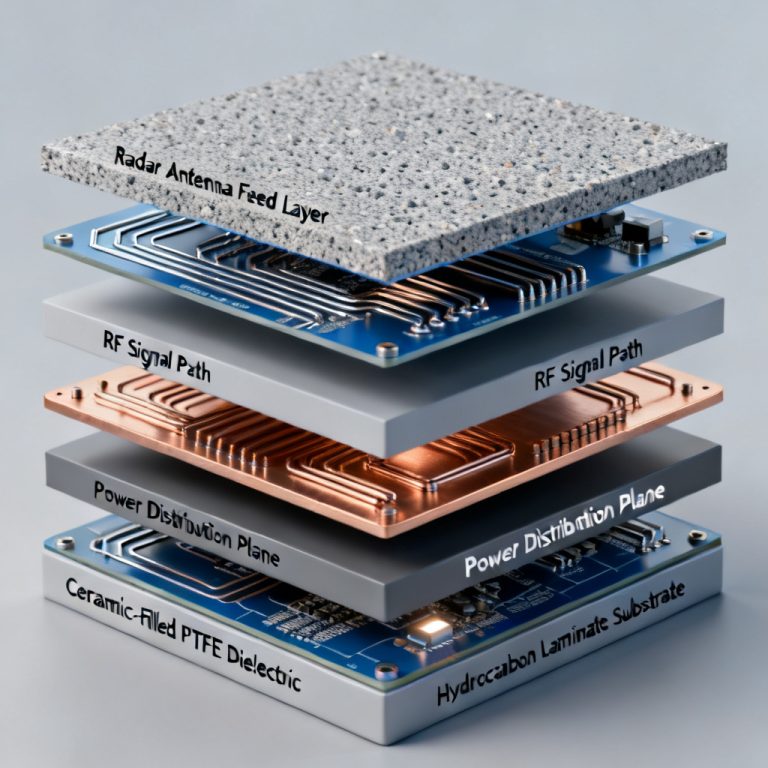
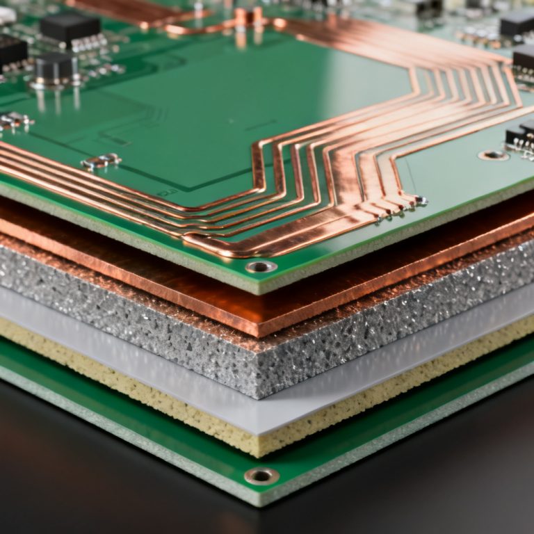
Stackup Engineering for High-Frequency Microwave PCBs
High-frequency microwave PCBs depend on precise stackup engineering to establish the electromagnetic baseline for controlled impedance, isolation, and thermal management. High-frequency microwave PCBs with poorly constructed stackups exhibit insertion loss degradation, impedance discontinuities, and unintended coupling between RF and digital domains.
Reference Plane Coupling in High-Frequency Microwave PCBs
High-frequency microwave PCBs require tight coupling between signal layers and reference planes to minimize loop inductance and suppress common-mode radiation. The dielectric thickness in high-frequency microwave PCBs should be selected to achieve target impedance while maintaining field containment. Thinner dielectrics in high-frequency microwave PCBs push parallel-plate resonance frequencies above the operating band, a critical consideration for mmWave designs.
Hybrid Multilayer Construction for High-Frequency Microwave PCBs
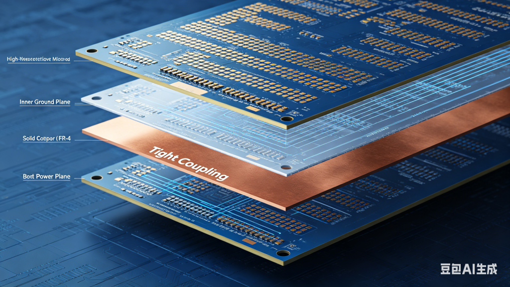
High-frequency microwave PCBs often employ hybrid constructions that use high-frequency laminates on RF layers while utilizing FR-4 or low-loss composites for control, power, and logic layers. This approach balances the performance requirements of high-frequency microwave PCBs with cost considerations for volume production.
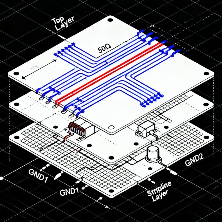
Transmission Line Design in High-Frequency Microwave PCBs
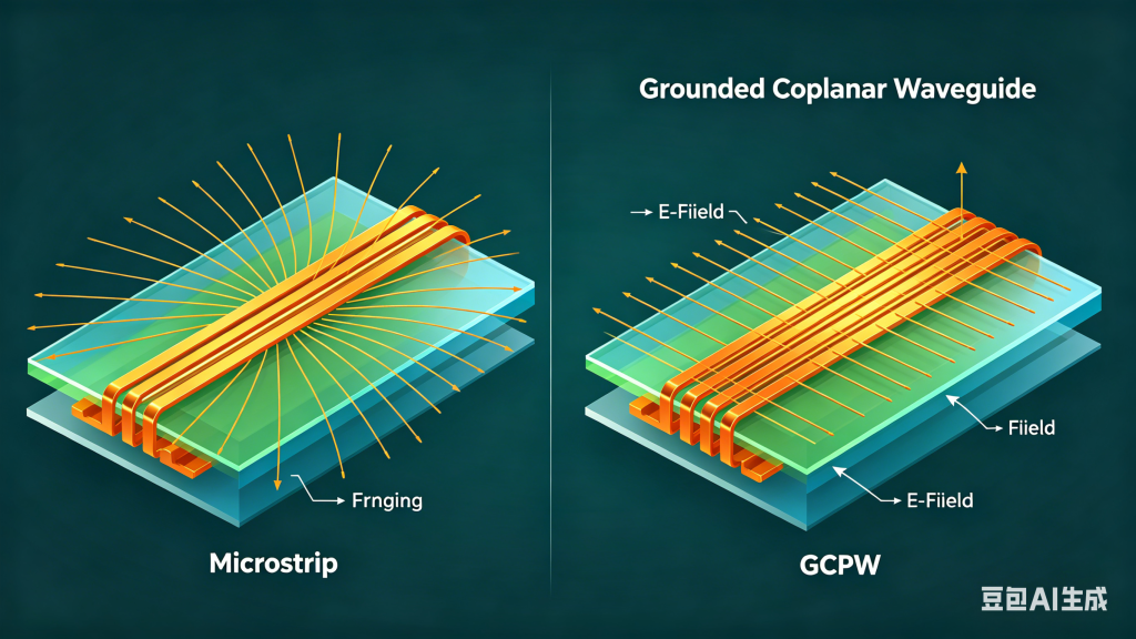
High-frequency microwave PCBs require transmission line structures that maintain controlled impedance and minimize radiation losses. At microwave frequencies, high-frequency microwave PCBs utilize microstrip, stripline, and grounded coplanar waveguide (GCPW) configurations, each with specific advantages depending on stackup constraints and isolation requirements.
Controlled Impedance in High-Frequency Microwave PCBs
Controlled impedance is the cornerstone of signal integrity in high-frequency microwave PCBs. The characteristic impedance of transmission lines in high-frequency microwave PCBs is determined by trace width, copper thickness, dielectric thickness, and dielectric constant. High-frequency microwave PCBs must maintain consistent trace geometry along the entire signal path to prevent reflections that degrade return loss and increase VSWR.
Critical Length Considerations for High-Frequency Microwave PCBs
High-frequency microwave PCBs require transmission line treatment when trace length exceeds the critical length threshold. For analog signals in high-frequency microwave PCBs, critical length lc = λₘ / 4, where λₘ is the maximum wavelength. For digital signals in mixed-signal high-frequency microwave PCBs, lc = tᵣ / (2 × tₚₔ). Traces in high-frequency microwave PCBs shorter than lc / 1.5 are considered shortlines and do not require controlled-impedance design.
Routing and Layout Guidelines for High-Frequency Microwave PCBs
High-frequency microwave PCBs demand routing practices that preserve signal integrity and minimize parasitic effects. High-frequency microwave PCBs operating at mmWave frequencies are particularly sensitive to corner discontinuities, trace width transitions, and coupling between adjacent RF paths.
Corner Treatment in High-Frequency Microwave PCBs
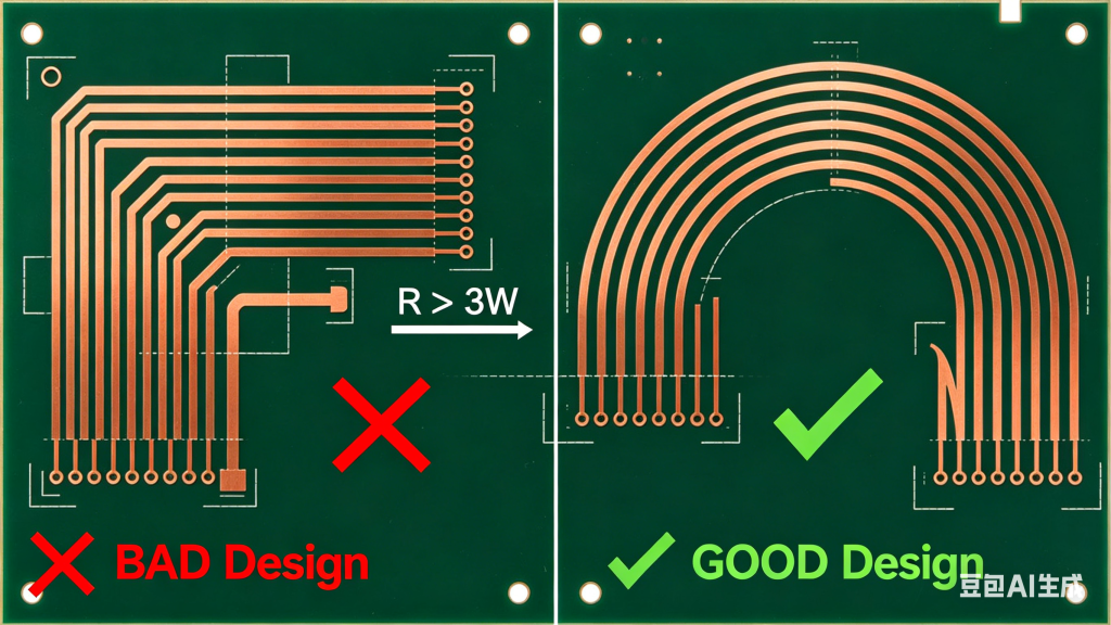
Sharp corners in high-frequency microwave PCBs generate electromagnetic field singularities that cause radiation loss and impedance discontinuities. High-frequency microwave PCBs should employ smooth, arc-shaped routing or 45° chamfered corners to maintain field continuity and minimize return loss. For high-frequency microwave PCBs operating above 30 GHz, arc routing is strongly preferred over chamfered corners.
Trace Width Transitions in High-Frequency Microwave PCBs
Abrupt trace width changes in high-frequency microwave PCBs create impedance transformers that reflect RF power and trigger signal radiation. High-frequency microwave PCBs should utilize tapered transitions to ensure smooth impedance continuity when routing from wide transmission lines to narrow component pads.
Spacing and Isolation in High-Frequency Microwave PCBs
High-frequency microwave PCBs require adequate spacing between RF traces and between RF and digital sections. The 3W rule (spacing ≥ 3 × trace width) provides a baseline for high-frequency microwave PCBs, but GHz designs typically require increased separation based on frequency and isolation specifications. High-frequency microwave PCBs should maintain at least 20 mm separation between digital and RF sections to prevent unwanted coupling.
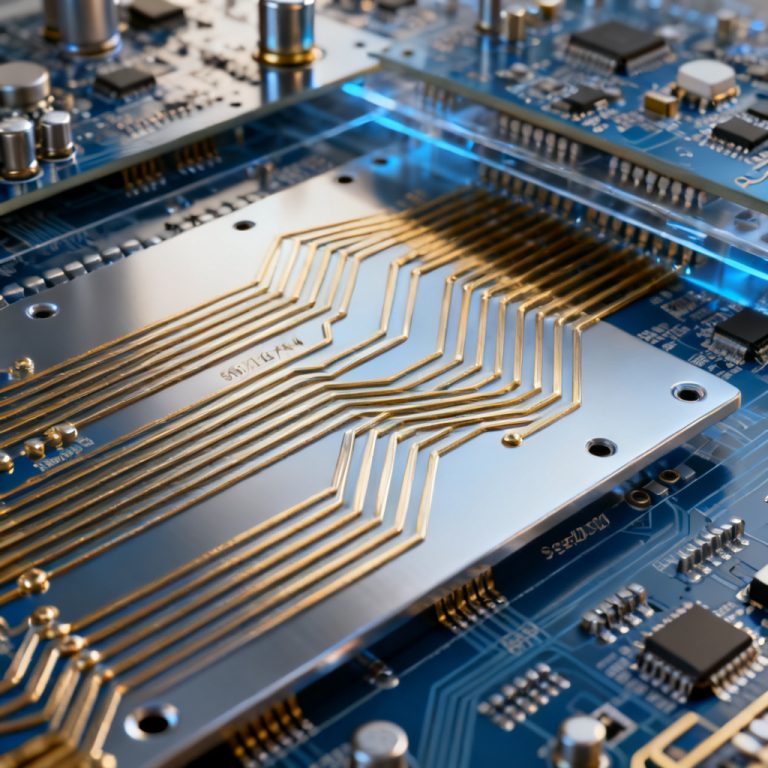
RF Via Engineering for High-Frequency Microwave PCBs
High-frequency microwave PCBs at mmWave frequencies require via designs that are treated as integral RF components, not merely mechanical interconnects. High-frequency microwave PCBs with poorly engineered vias suffer from resonant stubs, parasitic inductance, and mode conversion that degrade S-parameters and distort beamforming accuracy.
Back-Drilling for High-Frequency Microwave PCBs
High-frequency microwave PCBs benefit from back-drilling to remove unused via barrel sections that would otherwise create resonant stubs. In high-frequency microwave PCBs operating at 28-60 GHz, these stubs become resonant cavities that introduce impedance discontinuities and signal reflections.
Via Fencing in High-Frequency Microwave PCBs
High-frequency microwave PCBs employ via fencing—continuous rows of ground vias along transmission line edges—to provide electromagnetic shielding and prevent coupling between adjacent RF sections. The via-to-via spacing in high-frequency microwave PCBs should not exceed λ/20, where λ is the operating wavelength, to ensure effective field containment.
Grounding and Shielding Strategies for High-Frequency Microwave PCBs
High-frequency microwave PCBs require continuous, uninterrupted ground planes directly beneath all RF traces to provide consistent return current paths. High-frequency microwave PCBs with ground plane interruptions (slots, splits, or gaps) suffer from increased EMI and degraded signal integrity.
Advanced Shielding for High-Frequency Microwave PCBs
High-frequency microwave PCBs may require advanced shielding techniques beyond basic ground planes. Via fencing, electromagnetic bandgap (EBG) structures, and board-level metal shields provide enhanced isolation for high-frequency microwave PCBs in demanding applications such as phased-array antenna feeds and multi-channel transceivers.
Mixed-Signal Isolation in High-Frequency Microwave PCBs
High-frequency microwave PCBs containing both RF and digital circuitry must maintain physical separation between domains. For high-frequency microwave PCBs operating below approximately 1 GHz, star grounding with a single connection point may be employed; above this frequency, high-frequency microwave PCBs typically perform better with continuous ground planes and careful component placement.
Minimizing Discontinuities in High-Frequency Microwave PCBs
High-frequency microwave PCBs are susceptible to performance degradation from discontinuities and parasitic elements. Common sources in high-frequency microwave PCBs include sharp bends, abrupt transmission line transitions, vias in the RF path, and component pads that differ in width from connecting transmission lines.
Mitigation Strategies for High-Frequency Microwave PCBs
High-frequency microwave PCBs benefit from several discontinuity mitigation approaches: smooth arc routing, tapered transitions between transmission line types, minimized via usage, back-drilling when vias are unavoidable, and ground stitching vias to maintain consistent ground reference along the transmission path.
Thermal Management for High-Frequency Microwave PCBs
High-frequency microwave PCBs incorporating power amplifiers and high-power RF components require deliberate thermal management to ensure reliable operation and stable RF performance. High-frequency microwave PCBs without adequate thermal design may experience performance drift and reduced reliability under continuous RF load.
Thermal Conductivity in High-Frequency Microwave PCB Materials
| Property | Rogers RO4003C | Taconic TLX-8 | Relevance to High-Frequency Microwave PCBs |
|---|---|---|---|
| Thermal Conductivity (W/m·K) | 0.71 | 0.45 | Higher values improve heat dissipation in high-frequency microwave PCBs |
| Z-Axis CTE (ppm/°C) | 11 | 16 | Lower CTE improves reliability of high-frequency microwave PCBs under thermal cycling |
| Glass Transition Temp (Tg) | >280°C | >220°C | Higher Tg supports higher operating temperatures in high-frequency microwave PCBs |
Thermal Management Techniques for High-Frequency Microwave PCBs
High-frequency microwave PCBs utilize thermal via arrays beneath heat-generating components to conduct heat to internal copper planes or the opposite board side. High-frequency microwave PCBs may also employ copper pours, heavy copper (2 oz or greater), metal-core construction, or provisions for active cooling integration.
mmWave-Specific Design for High-Frequency Microwave PCBs
High-frequency microwave PCBs for mmWave applications (30-300 GHz) face unique challenges including spurious-wave-mode propagation, increased conductor and radiation losses, unwanted resonance, and dispersion. High-frequency microwave PCBs at these frequencies require thinner dielectrics and tighter manufacturing tolerances than lower-frequency designs.
Manufacturing Tolerances in mmWave High-Frequency Microwave PCBs
High-frequency microwave PCBs operating at mmWave frequencies are significantly more sensitive to fabrication tolerances. A 28 GHz patch antenna on high-frequency microwave PCBs designed for 5.3 × 5.3 mm elements will suffer approximately 7% resonant frequency shift if fabricated at 5.45 × 5.45 mm due to standard PCB etching tolerances. High-frequency microwave PCBs for mmWave applications therefore require close collaboration with fabricators to establish achievable tolerance windows.
Land Pattern Optimization for High-Frequency Microwave PCBs
High-frequency microwave PCBs require optimized land patterns for mmWave components. The RF layer thickness and Dk of high-frequency microwave PCBs influence the shunt capacitance experienced by mounted RF filters, making board layout optimization around and under RF components essential for maintaining optimal VSWR.
Surface Finish Selection for High-Frequency Microwave PCBs
High-frequency microwave PCBs require careful surface finish selection due to the skin effect concentration of current at the conductor surface. At microwave frequencies, high-frequency microwave PCBs with inappropriate surface finishes exhibit measurable degradation in insertion loss, return loss, and passive intermodulation performance.
Surface Finish Options for High-Frequency Microwave PCBs
| Frequency Range | Recommended Finish for High-Frequency Microwave PCBs | Considerations |
|---|---|---|
| Below 3 GHz | HASL or ENIG | HASL cost-effective for non-critical high-frequency microwave PCBs; ENIG for reliability |
| 3-10 GHz | ENIG or Immersion Silver | Nickel loss becomes measurable in high-frequency microwave PCBs |
| 10-30 GHz | Immersion Silver | Minimizes nickel barrier loss in high-frequency microwave PCBs |
| Above 30 GHz | Immersion Silver or Bare Copper with OSP | Eliminates nickel entirely for lowest-loss high-frequency microwave PCBs |
Surface Roughness Impact on High-Frequency Microwave PCBs
Copper surface roughness increases the effective current path length in high-frequency microwave PCBs, adding to conductor loss. RMS roughness values above 1 μm can increase attenuation by 20-40% in high-frequency microwave PCBs operating at mmWave frequencies. High-frequency microwave PCBs requiring lowest insertion loss should specify smooth copper (low-profile or reverse-treated foils) for RF layers.
Impedance Matching for High-Frequency Microwave PCBs
High-frequency microwave PCBs require impedance matching networks to minimize signal reflections and ensure maximum power transfer. High-frequency microwave PCBs employ quarter-wave transformers, tapered lines, stub matching networks, or lumped-element matching networks depending on frequency range and bandwidth requirements.
Matching Network Design for High-Frequency Microwave PCBs
High-frequency microwave PCBs benefit from simulation-based matching network design. Quarter-wave transformers provide simple narrow-band matching for high-frequency microwave PCBs, while tapered lines offer broadband impedance transitions. High-frequency microwave PCBs operating at frequencies where discrete components remain effective may utilize L, Pi, or T network topologies with surface-mount inductors and capacitors.
DFM and Manufacturing for High-Frequency Microwave PCBs
High-frequency microwave PCBs require tighter manufacturing tolerances than standard PCBs. High-frequency microwave PCBs demand registration tolerance of 2 mils or better, controlled copper thickness variation within ±10%, and precise etching control to maintain trace width and gap dimensions critical for impedance control.
IPC Standards for High-Frequency Microwave PCBs
High-frequency microwave PCBs should reference applicable IPC standards to ensure consistent quality and performance:
- IPC-4101: Base material specification for high-frequency microwave PCBs
- IPC-4103: High-speed/high-frequency material specification for high-frequency microwave PCBs
- IPC-6018: Qualification and performance specification for high-frequency microwave PCBs
- IPC-2228: Sectional design standard for high-frequency microwave PCBs
Fabrication Collaboration for High-Frequency Microwave PCBs
High-frequency microwave PCBs require close collaboration between design and fabrication teams. Stackup planning for high-frequency microwave PCBs should include verification of material availability, impedance calculation validation, and establishment of achievable tolerance windows. High-frequency microwave PCBs for mmWave applications benefit from pre-production engineering reviews to identify potential fabrication challenges.
Simulation and Validation of High-Frequency Microwave PCBs
High-frequency microwave PCBs require simulation throughout the design process to validate performance before fabrication. High-frequency microwave PCBs benefit from transmission line calculations using impedance solvers, signal integrity analysis of critical RF paths, full-wave electromagnetic simulation of complex structures, and thermal simulation of high-power sections.
Key Performance Parameters for High-Frequency Microwave PCBs
| Parameter | Definition | Target for High-Frequency Microwave PCBs |
|---|---|---|
| Insertion Loss (S21) | Signal attenuation through path | Minimize per application link budget for high-frequency microwave PCBs |
| Return Loss (S11) | Impedance matching quality | >10 dB or >15 dB for high-frequency microwave PCBs |
| Isolation (S21 between ports) | Coupling between adjacent paths | >30 dB for most high-frequency microwave PCBs |
| VSWR | Voltage Standing Wave Ratio | <2.0:1 for typical high-frequency microwave PCBs |
Complete Design Workflow for High-Frequency Microwave PCBs
High-frequency microwave PCBs follow a systematic 16-step design workflow adapted from established microwave PCB methodologies:
| Step | Activity for High-Frequency Microwave PCBs | Key Deliverables |
|---|---|---|
| 1 | Define design requirements | Frequency, power, impedance targets for high-frequency microwave PCBs |
| 2 | Select substrate materials | Material datasheets, Dk/Df verification for high-frequency microwave PCBs |
| 3 | Design layer stackup | Stackup diagram, layer assignments for high-frequency microwave PCBs |
| 4 | Calculate trace geometries | Trace widths validated with fabricator for high-frequency microwave PCBs |
| 5 | Design transmission lines | Microstrip/stripline/GCPW for high-frequency microwave PCBs |
| 6 | Implement impedance matching | Matching networks for high-frequency microwave PCBs |
| 7 | Minimize discontinuities | Arc routing, tapered transitions in high-frequency microwave PCBs |
| 8 | Implement grounding | Continuous planes, via fencing in high-frequency microwave PCBs |
| 9 | Optimize component placement | Parasitic minimization, isolation for high-frequency microwave PCBs |
| 10 | Manage thermal requirements | Thermal vias, copper pours for high-frequency microwave PCBs |
| 11 | Select surface finish | Immersion silver or ENIG for high-frequency microwave PCBs |
| 12 | Perform simulation | EM, SI, thermal analysis for high-frequency microwave PCBs |
| 13 | DFM review | Material availability, stackup feasibility for high-frequency microwave PCBs |
| 14 | Document stackup and fabrication | Complete requirements for high-frequency microwave PCBs |
| 15 | Fabrication and assembly | IPC-6018 quality control for high-frequency microwave PCBs |
| 16 | Testing and validation | S-parameter, functional, environmental testing for high-frequency microwave PCBs |
Conclusion: Key Principles for High-Frequency Microwave PCBs
High-frequency microwave PCBs require a comprehensive understanding of electromagnetic principles, material science, and manufacturing processes. The following key principles summarize essential guidance for high-frequency microwave PCBs:
- High-frequency microwave PCBs require clear requirements documentation before layout begins.
- High-frequency microwave PCBs depend on stable, low-Dk, low-Df laminate selection matched to application requirements.
- High-frequency microwave PCBs performance is established by precise stackup engineering for controlled impedance and isolation.
- High-frequency microwave PCBs must maintain consistent characteristic impedance along all transmission line paths.
- High-frequency microwave PCBs should keep traces shorter than λ/4 to avoid distributed effects, or model longer traces explicitly as transmission lines.
- High-frequency microwave PCBs benefit from smooth arc routing, tapered transitions, and minimized discontinuities.
- High-frequency microwave PCBs require continuous ground planes, via fencing, and proper isolation between circuit domains.
- High-frequency microwave PCBs at mmWave frequencies treat via design as part of the RF chain, with back-drilling and optimized geometries.
- High-frequency microwave PCBs require surface finishes selected based on operating frequency to minimize conductor loss.
- High-frequency microwave PCBs with high-power sections demand deliberate thermal management.
- High-frequency microwave PCBs for mmWave applications are less forgiving of manufacturing variations, requiring close fabrication collaboration.
- High-frequency microwave PCBs benefit from reference to industry standards including IPC-4101, IPC-2228, and IPC-6018.
Frequently Asked Questions About High-Frequency Microwave PCBs
What are high-frequency microwave PCBs used for?
High-frequency microwave PCBs are used in applications operating at frequencies from several hundred MHz to beyond 86 GHz, including 5G FR2 base stations and user equipment, automotive radar systems (24 GHz, 77 GHz), satellite communication payloads, phased-array antennas, high-resolution sensing, and advanced test and measurement equipment. High-frequency microwave PCBs provide the controlled-impedance, low-loss signal paths required for these demanding RF and mmWave applications.
What materials are best for high-frequency microwave PCBs?
High-frequency microwave PCBs typically utilize specialized laminates with stable dielectric constant (Dk) and low dissipation factor (Df). Rogers materials (RO4350B, RO3003, RO4835, RT/duroid 5880) are industry standards for high-frequency microwave PCBs, offering proven performance across frequency ranges. Taconic laminates (RF-35, TLY-5) provide alternatives with specific performance advantages for high-frequency microwave PCBs in ultra-low-loss or aerospace applications. The optimal material for high-frequency microwave PCBs depends on operating frequency, power handling, thermal requirements, and cost constraints.
Why is controlled impedance important for high-frequency microwave PCBs?
Controlled impedance is essential for high-frequency microwave PCBs because impedance discontinuities cause signal reflections that degrade return loss, increase insertion loss, and distort phase response. High-frequency microwave PCBs operating at mmWave frequencies are particularly sensitive to impedance variations, which can shift filter responses, detune antenna matching, and compromise beamforming accuracy in phased-array systems. High-frequency microwave PCBs maintain consistent characteristic impedance through precise trace geometry control and stable dielectric materials.
How does surface finish affect high-frequency microwave PCBs?
Surface finish directly impacts conductor loss in high-frequency microwave PCBs due to the skin effect, which concentrates high-frequency current near the conductor surface. High-frequency microwave PCBs operating above 10 GHz benefit from immersion silver finishes, which eliminate the loss contribution from nickel barrier layers present in ENIG. High-frequency microwave PCBs above 30 GHz may require bare copper with OSP or silver finishes to achieve lowest possible insertion loss. HASL finishes are generally not recommended for critical RF paths in high-frequency microwave PCBs.
What manufacturing tolerances are required for high-frequency microwave PCBs?
High-frequency microwave PCBs require tighter manufacturing tolerances than standard PCBs, including registration tolerance of 2 mils or better, copper thickness control within ±10%, and precise etching control for trace width and gap dimensions. High-frequency microwave PCBs for mmWave applications are particularly sensitive to tolerance variations—a 0.15 mm etching variation can shift a 28 GHz antenna resonant frequency by approximately 7%. High-frequency microwave PCBs should be developed in close collaboration with fabricators to establish achievable tolerance windows.