Mastering High Voltage PCB Design requires a deep understanding of creepage, clearance, and partial discharge. This guide provides expert insights into these critical parameters for reliable, safe, and long-lasting power electronics, industrial inverters, and EV chargers. We cover IPC-2221 and IEC 60950 standards, material selection, and practical design rules to prevent arcing, tracking, and insulation breakdown.

1. Clearance in High Voltage PCB Design
1.1 What is Clearance?
Clearance is the shortest distance through air between two conductive parts. It is a measure of air insulation under normal atmospheric conditions, critical for High Voltage PCB Design to prevent immediate arcing.
1.2 Why Clearance Matters for High Voltage PCB Design
The primary threat to clearance is dielectric breakdown of air. When the electric field exceeds ~3 kV/mm at sea level, a spark can jump across the gap. This is an immediate, catastrophic failure in any High Voltage PCB Design.
1.3 Key Factors Affecting Clearance in High Voltage PCB Design
From top sources, we consolidate these factors: Peak Working Voltage (Vpk), Altitude, Pollution Degree (PD 1, 2, 3), and Transient Overvoltages. For High Voltage PCB Design, always use the peak voltage and highest pollution degree.
1.4 Standard Calculation Methods for High Voltage PCB Design Clearance
IPC-2221A and IEC 60950-1 provide formulas and tables. For example, for 1000Vpk: PD1 requires ~3.0 mm, PD2 requires ~6.0 mm, and PD3 requires ~12.0 mm clearance. A slot or hole in the PCB can increase effective clearance distance.
| Peak Voltage (Vpk) | Pollution Degree 1 | Pollution Degree 2 | Pollution Degree 3 |
|---|---|---|---|
| 300V | 1.5 mm | 3.0 mm | 6.0 mm |
| 600V | 3.0 mm | 6.0 mm | 12.0 mm |
| 1000V | 6.0 mm | 12.0 mm | 20.0 mm |

2. Creepage in High Voltage PCB Design
2.1 What is Creepage?
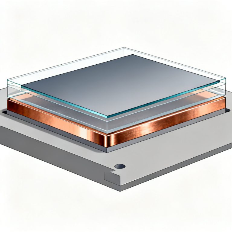
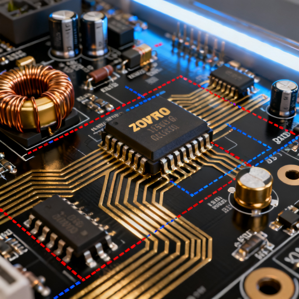
Creepage is the shortest distance along the surface of the insulating material between two conductive parts. Unlike clearance, creepage measures the path on the board material, a key concept in High Voltage PCB Design.
2.2 Why Creepage is More Dangerous in High Voltage PCB Design
Creepage failure is a gradual process called tracking. Contamination creates a conductive path. Over time, leakage currents carbonize the epoxy resin, leading to permanent short-circuit and fire. This makes creepage a critical focus in High Voltage PCB Design.
2.3 Key Factors Affecting Creepage in High Voltage PCB Design
RMS Working Voltage, Comparative Tracking Index (CTI) of the PCB material, Pollution Degree, and Material Group. For High Voltage PCB Design, choose materials with CTI Group I (≥600V) for best performance.
2.4 Standard Creepage Tables for High Voltage PCB Design
IEC 60950-1 Table 2L provides minimum creepage distances. For 1000V RMS, PD2: Material Group I requires ~8.0 mm, Group II requires ~10.0 mm, Group IIIa requires ~12.5 mm. Creepage is almost always larger than clearance for the same voltage.
2.5 How to Increase Creepage in High Voltage PCB Design
Add a routed slot, use a thick solder mask dam, increase board thickness, or apply conformal coating. These techniques improve reliability in High Voltage PCB Design.

3. Partial Discharge in High Voltage PCB Design
3.1 What is Partial Discharge?
Partial Discharge (PD) is a localized electrical discharge that only partially bridges the insulation. It occurs inside small voids or at copper edges within the PCB laminate. For High Voltage PCB Design above 500V RMS, PD is often the limiting factor.
3.2 Why PD is Critical for High Voltage PCB Design
PD erodes insulation over time, generating ozone and nitric acid. This chemical attack leads to eventual flashover. Understanding PD is essential for long-term reliability in High Voltage PCB Design.
3.3 Key Parameters for PD in High Voltage PCB Design
PDIV (Partial Discharge Inception Voltage), PDEV (Extinction Voltage), and Charge Magnitude (pC). For high-reliability High Voltage PCB Design, limit PD to <10 pC at 1.5x operating voltage.
3.4 Causes of PD in High Voltage PCB Design
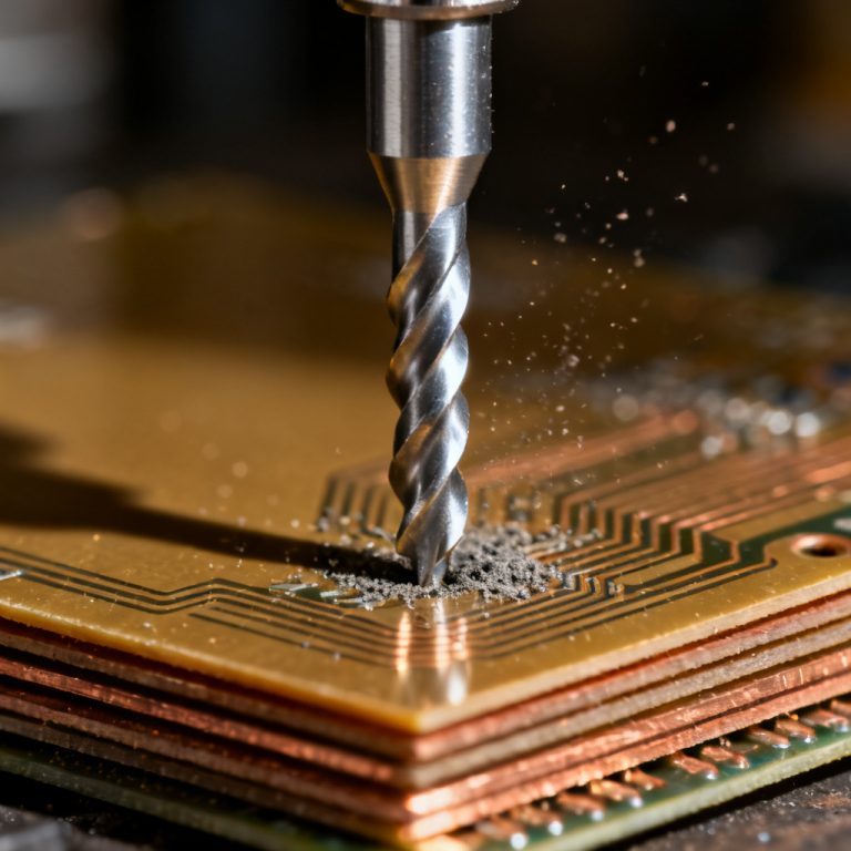
Voids in the laminate, sharp edges on copper, thin dielectric layers, poor plating in vias, and contamination. These are common issues in High Voltage PCB Design that must be addressed.
3.5 Design Rules to Minimize PD in High Voltage PCB Design
Use high voltage laminates (e.g., Isola 370HR, Rogers 4350B), increase inner layer spacing to >0.3mm for 1000V, avoid 90° corners, use teardrop pads, add guard rings, and specify PD testing. These rules are critical for successful High Voltage PCB Design.
3.6 PD vs. Clearance/Creepage: A Summary Table for High Voltage PCB Design
| Parameter | Clearance | Creepage | Partial Discharge |
|---|---|---|---|
| Path | Through air | Along board surface | Inside insulation/voids |
| Failure Mode | Instant arcing | Slow tracking / carbonization | Gradual erosion / breakdown |
| Primary Threat | Peak voltage, altitude | RMS voltage, contamination, CTI | High voltage, voids, sharp edges |
| Key Standard | IEC 60664, IPC-2221 | IEC 60950, IPC-2221 | IEC 60270, IPC-9592 |
| Design Focus | Physical distance | Material selection & surface path | Material quality & edge geometry |

4. Practical Design Checklist for High Voltage PCB Design
To ensure your High Voltage PCB Design meets safety and reliability standards, follow this checklist: define the environment (PD, altitude), calculate peak and RMS voltages, select material CTI, determine minimum distances for clearance and creepage, design for PD suppression, consider conformal coating, and prototype with PD testing.
5. FAQ: High Voltage PCB Design
What is the difference between creepage and clearance in High Voltage PCB Design?
Clearance is the shortest distance through air between conductors, while creepage is the shortest distance along the surface of the PCB material. Both are critical in High Voltage PCB Design to prevent arcing and tracking.
How do I calculate clearance for my High Voltage PCB Design?
Use IPC-2221 Table 6-1 or IEC 60664-1. For High Voltage PCB Design, always use the peak working voltage and consider altitude and pollution degree.
What is Partial Discharge and why is it important in High Voltage PCB Design?
Partial Discharge (PD) is a localized discharge that erodes insulation over time. It is a key concern in High Voltage PCB Design above 500V RMS, as it can lead to premature failure.
How can I reduce Partial Discharge in my High Voltage PCB Design?
Use high-quality laminates with low void content, avoid sharp copper edges, increase inner layer spacing, and specify PD testing. These practices improve reliability in High Voltage PCB Design.
What is the best material for High Voltage PCB Design?
Materials with high CTI (Group I or II) and low void content, such as high-Tg FR-4, Isola 370HR, or Rogers 4350B, are recommended for High Voltage PCB Design.