This comprehensive guide explores High Thermal Conductivity PCB solutions using aluminum, copper, and ceramic substrates for superior heat dissipation in power electronics, LED lighting, and automotive applications.
High Thermal Conductivity PCB Basics
Thermal Conductivity Fundamentals for High Thermal Conductivity PCB
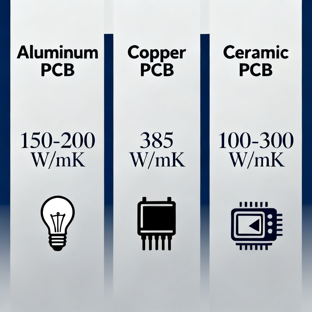
Thermal conductivity (W/m·K) quantifies a material’s ability to conduct heat. For High Thermal Conductivity PCB, higher values mean faster heat transfer from components like LEDs and power transistors. Standard FR-4 offers ~0.3 W/m·K, while aluminum MCPCBs range 1–3 W/m·K, and ceramic substrates exceed 200 W/m·K.
Why Standard FR-4 Fails for High Thermal Conductivity PCB Applications
FR-4 is a poor thermal conductor. In high-power designs, heat accumulates, reducing LED efficacy, accelerating semiconductor aging, causing thermal runaway, and leading to solder joint failure. Industries like automotive lighting and medical lasers mandate High Thermal Conductivity PCB solutions.
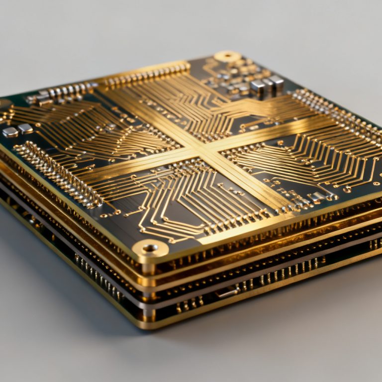
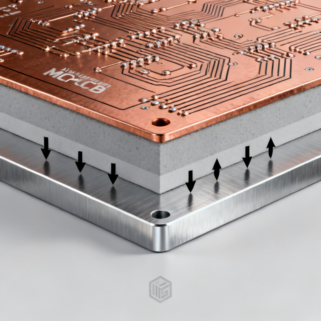
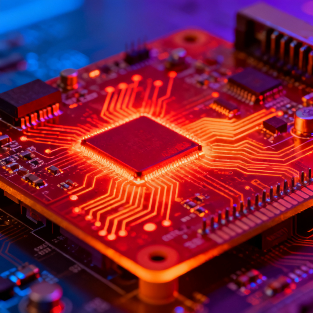
Aluminum High Thermal Conductivity PCB
Construction and Thermal Mechanism of Aluminum High Thermal Conductivity PCB
An aluminum High Thermal Conductivity PCB comprises a copper circuit layer, a thermally conductive dielectric (1.0–3.0 W/m·K), and an aluminum base (200–220 W/m·K). The dielectric is the thermal bottleneck, but the aluminum base acts as a large-area heatsink.
Key Advantages of Aluminum High Thermal Conductivity PCB
- Cost-effective for high-volume production
- Lightweight (one-third density of copper)
- Excellent mechanical rigidity
- Good corrosion resistance
Typical Applications for Aluminum High Thermal Conductivity PCB
- LED lighting (streetlights, automotive headlamps)
- Power supply modules
- Motor controllers
- Battery management systems
Design Considerations for Aluminum High Thermal Conductivity PCB
- Dielectric thickness: thinner improves thermal performance but reduces voltage isolation
- Copper weight: heavier copper (e.g., 4 oz) reduces resistive losses
- Thermal vias: enhance heat transfer to aluminum base
Copper High Thermal Conductivity PCB
Why Copper Outperforms Aluminum in High Thermal Conductivity PCB
Copper has thermal conductivity ~385–400 W/m·K, nearly double aluminum. Copper-core High Thermal Conductivity PCB is premier for extreme heat dissipation.
Construction Variants of Copper High Thermal Conductivity PCB
- Copper-core MCPCB: solid copper base replaces aluminum
- Embedded copper coin: localized thermal path under hot components
- Heavy copper PCB: thick copper layers for high current and thermal spreading
Key Advantages of Copper High Thermal Conductivity PCB
- Highest thermal conductivity among metal substrates
- Excellent heat spreading
- Superior current-carrying capacity
- Better solderability for high-temperature environments
Typical Applications for Copper High Thermal Conductivity PCB
- High-power LED arrays (100W+ COB LEDs)
- IGBT modules and power inverters
- RF power amplifiers
- Electric vehicle traction inverters
Design Considerations for Copper High Thermal Conductivity PCB
- Weight: three times heavier than aluminum
- Cost: 2–3x more expensive than aluminum alternatives
- Thermal expansion mismatch: requires careful design
- Dielectric selection: low-thermal-resistance dielectrics essential
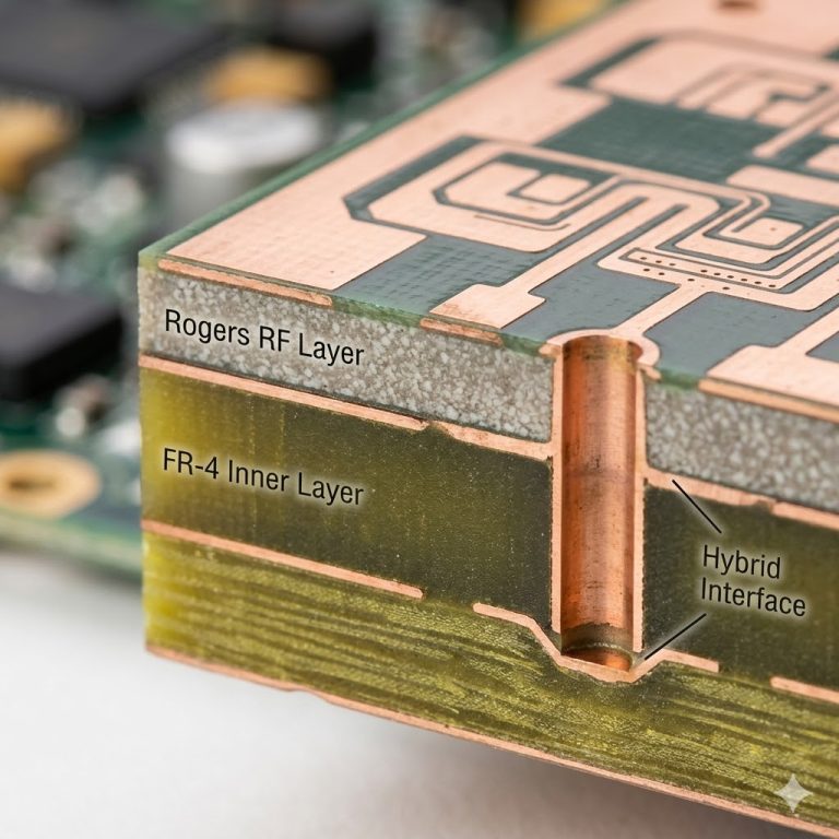
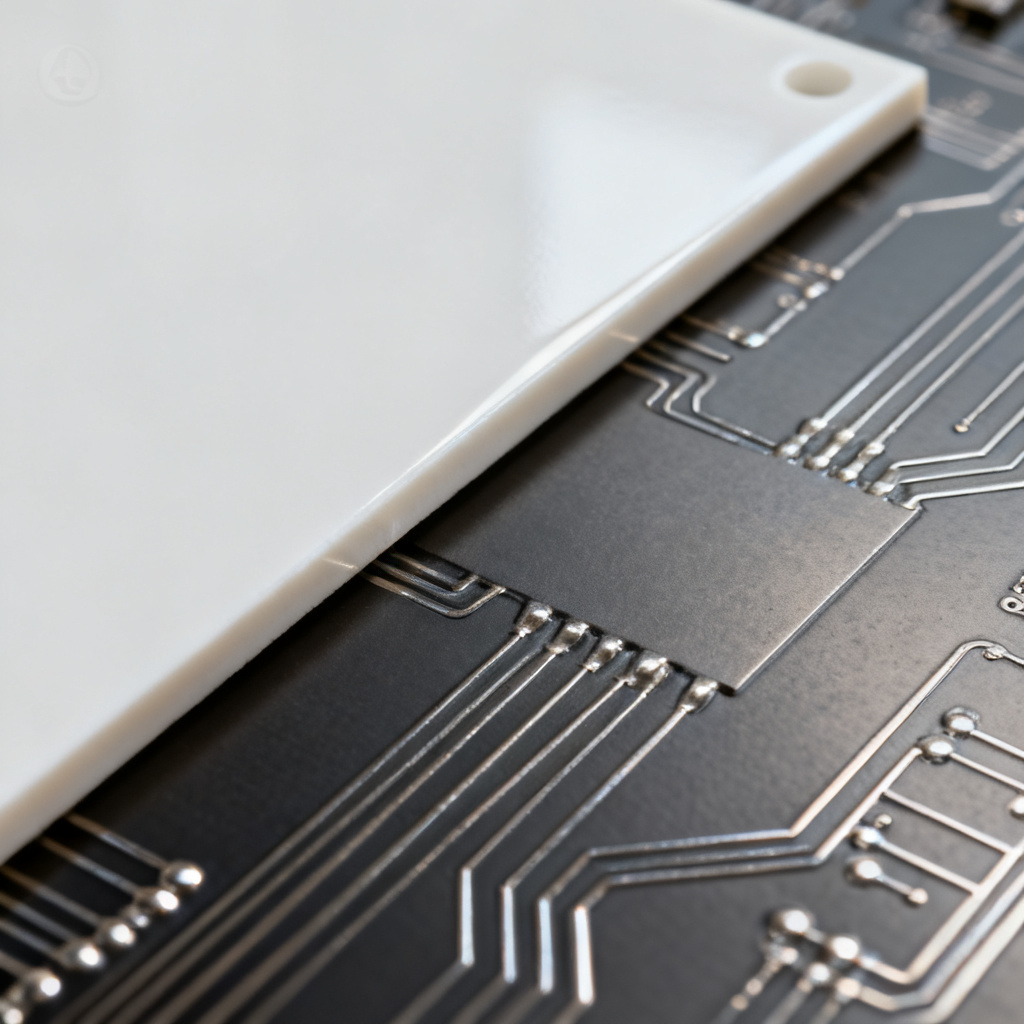
Ceramic High Thermal Conductivity PCB
Unique Properties of Ceramic High Thermal Conductivity PCB
Ceramic High Thermal Conductivity PCB substrates are non-metallic, thermally conductive, and electrically insulating. Common materials: Alumina (20–30 W/m·K), Aluminum Nitride (170–200 W/m·K), Beryllium Oxide (250–300 W/m·K, toxic), Silicon Nitride (90–120 W/m·K).
Construction and Processing of Ceramic High Thermal Conductivity PCB
- Thick-film technology: conductive pastes screen-printed and fired
- Direct Bond Copper (DBC): copper foil bonded to ceramic
- Active Metal Brazing (AMB): stronger bond for Si₃N₄
Key Advantages of Ceramic High Thermal Conductivity PCB
- Inherent electrical insulation, no dielectric bottleneck
- Extremely high thermal conductivity (AlN comparable to aluminum)
- High temperature resistance (300°C+)
- Excellent CTE match to silicon
- Chemical inertness
Typical Applications for Ceramic High Thermal Conductivity PCB
- High-power LED modules (UV and IR)
- Power semiconductor modules (IGBT, SiC MOSFET)
- RF and microwave circuits
- Medical devices
- Oil and gas downhole electronics
Design Considerations for Ceramic High Thermal Conductivity PCB
- Cost: 5–10x aluminum PCBs
- Brittleness: requires careful handling
- Limited size: typically 4–6 inches square
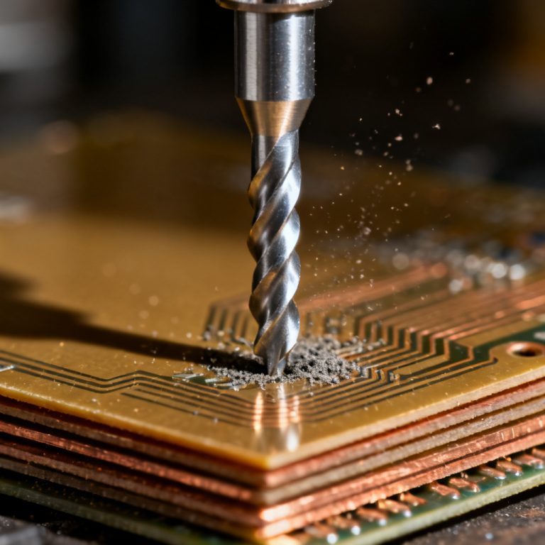
- Laser drilling for vias
- High-performance TIM needed
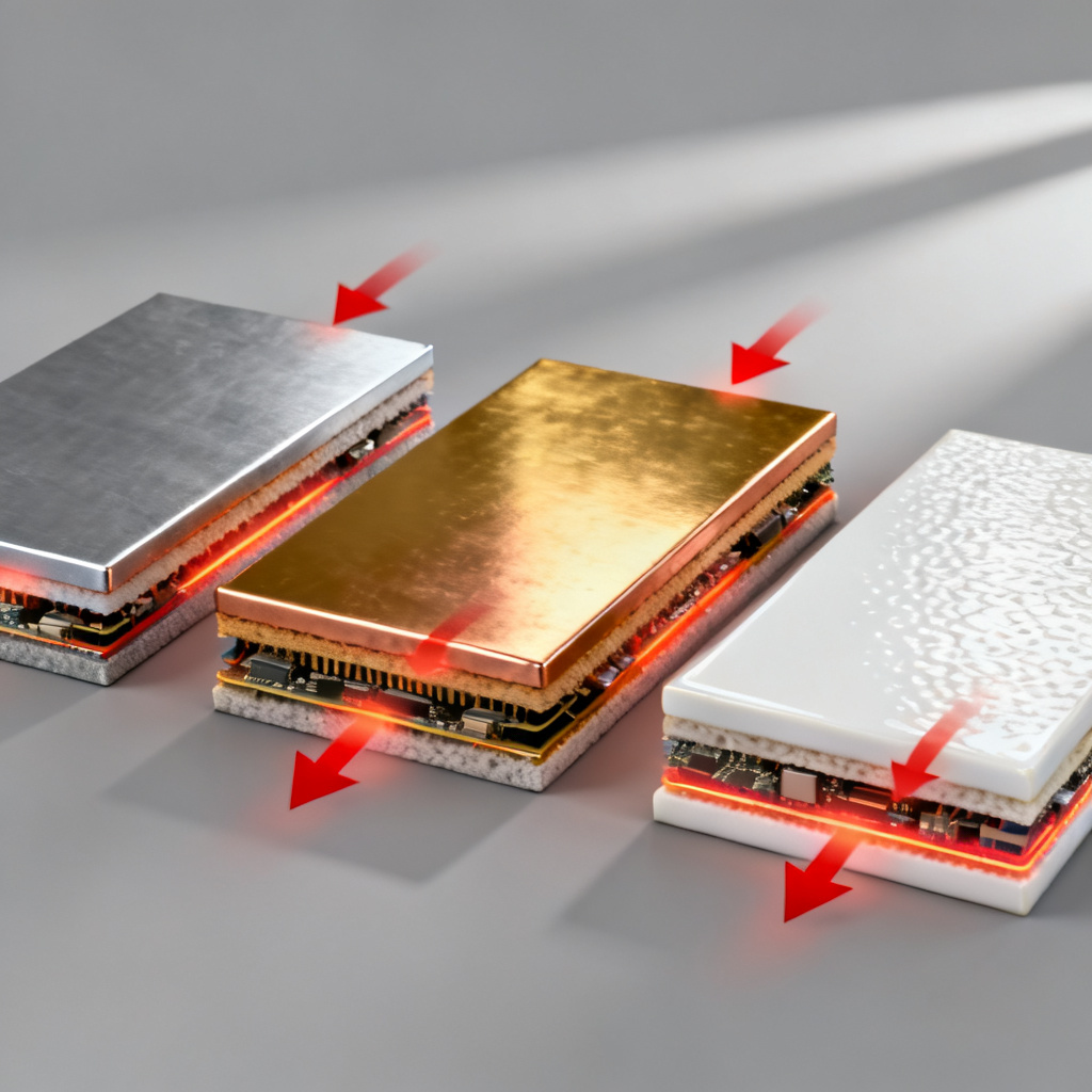
High Thermal Conductivity PCB Comparative Analysis
| Parameter | Aluminum High Thermal Conductivity PCB | Copper High Thermal Conductivity PCB | Ceramic High Thermal Conductivity PCB (AlN) |
|---|---|---|---|
| Thermal Conductivity (W/m·K) | 1–3 (dielectric limited) | 385–400 (base) | 170–200 (substrate) |
| Electrical Insulation | Yes (via dielectric) | Yes (via dielectric) | Inherent |
| Max Operating Temperature | ~140°C | ~140°C | 300°C+ |
| Weight | Light | Heavy | Moderate |
| Relative Cost | Low | Medium-High | High |
| CTE Match to Silicon | Poor | Good | Excellent |
| Mechanical Robustness | Excellent | Excellent | Brittle |
| Typical Application | General LED lighting | High-power LEDs, IGBT | Power modules, RF |
When to Choose Aluminum High Thermal Conductivity PCB
- Budget is primary constraint
- Moderate thermal loads (< 50 W/cm²)
- Large board sizes required
- Weight-sensitive applications
When to Choose Copper High Thermal Conductivity PCB
- Extreme thermal loads (> 100 W/cm²)
- High current density (50+ amps)
- Need for superior heat spreading
- Reliability in harsh thermal cycling
When to Choose Ceramic High Thermal Conductivity PCB
- Need for electrical isolation without dielectric bottleneck
- High-temperature environment (> 150°C)
- Direct die attach (no TIM)
- RF or high-frequency circuits
- Miniaturization with higher power density
Design Rules for High Thermal Conductivity PCB
Thermal Via Optimization for High Thermal Conductivity PCB
- Use filled vias (copper or silver epoxy)
- Place vias under heat sources in grid pattern (0.5–1.0 mm spacing)
- Minimize via diameter (0.3–0.5 mm)
- For ceramic, laser-drilled microvias required
Dielectric Layer Selection for High Thermal Conductivity PCB
- Choose dielectrics with thermal conductivity ≥ 1.5 W/m·K
- Thinner dielectric (25–50 µm) improves thermal performance
- For high voltage (>1000V), use thicker dielectric (100–150 µm)
Copper Thickness and Trace Design for High Thermal Conductivity PCB
- Use heavy copper (2–6 oz) for high-current and thermal spreading
- Keep thermal traces wide and short
- Avoid sharp corners; use rounded thermal pads
Component Placement for High Thermal Conductivity PCB
- Place heat-generating components close to PCB edge
- Use symmetrical placement to balance thermal expansion
- Consider thermal pads or copper coins for hot spots
Thermal Interface Material (TIM) for High Thermal Conductivity PCB
- Use high-performance TIM (≥ 3 W/m·K)
- Ensure uniform pressure to minimize air gaps
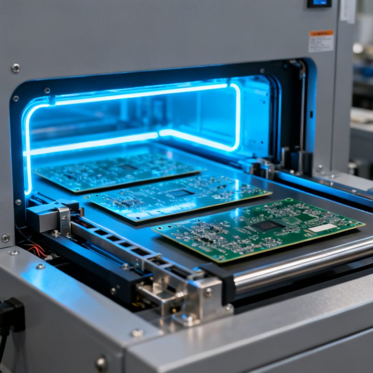
Manufacturing and Quality for High Thermal Conductivity PCB
Surface Finish Options for High Thermal Conductivity PCB
- HASL: cost-effective but uneven surface
- ENIG: flat surface, good for fine-pitch components
- OSP: low cost, limited shelf life
- Immersion Silver: good thermal conductivity, sulfur-sensitive
Testing and Validation for High Thermal Conductivity PCB
- Thermal imaging: verify temperature distribution
- Thermal resistance measurement: use T3Ster
- Thermal cycling: -40°C to +125°C for 1000 cycles
- Dielectric strength test per IPC-4101
Certifications for High Thermal Conductivity PCB
- UL 94 V-0: flame retardancy
- IPC-6012: qualification specification
- RoHS/REACH: environmental compliance
Future Trends in High Thermal Conductivity PCB
Graphene-Enhanced Dielectrics for High Thermal Conductivity PCB
Graphene (thermal conductivity ~5000 W/m·K) may achieve 5–10 W/m·K in MCPCB dielectrics.
Diamond-Based Substrates for High Thermal Conductivity PCB
Synthetic diamond films (>2000 W/m·K) are explored for defense and aerospace.
3D-Printed Thermal Structures for High Thermal Conductivity PCB
Additive manufacturing enables embedded cooling channels and conformal vias.
Integrated Heatsink PCBs for High Thermal Conductivity PCB
New designs integrate fins or microchannels directly into the substrate.
Conclusion: Selecting the Right High Thermal Conductivity PCB
Choosing between aluminum, copper, and ceramic High Thermal Conductivity PCB depends on thermal, electrical, mechanical, and cost requirements. Aluminum works for cost-sensitive LED and power applications. Copper excels when heat dissipation is paramount. Ceramic is indispensable for high-temperature, high-voltage, or high-frequency designs. Understanding design rules ensures reliable performance and extended lifespan.
FAQ: High Thermal Conductivity PCB
What is a High Thermal Conductivity PCB?
A High Thermal Conductivity PCB uses substrates like aluminum, copper, or ceramic to efficiently transfer heat away from components, preventing overheating in power electronics and LED lighting.
Which High Thermal Conductivity PCB material is best for LED lighting?
Aluminum High Thermal Conductivity PCB is most cost-effective for general LED lighting, while copper or ceramic is preferred for high-power or UV LEDs.
Can a High Thermal Conductivity PCB replace a heatsink?
No, a High Thermal Conductivity PCB improves heat spreading but typically still requires a heatsink for extreme thermal loads.
What is the thermal conductivity of ceramic High Thermal Conductivity PCB?
Aluminum Nitride ceramic High Thermal Conductivity PCB offers 170–200 W/m·K, while Alumina provides 20–30 W/m·K.
Why is dielectric important in High Thermal Conductivity PCB?
The dielectric layer in metal-core High Thermal Conductivity PCB provides electrical insulation but is the primary thermal bottleneck, so selecting a high-conductivity dielectric is critical.