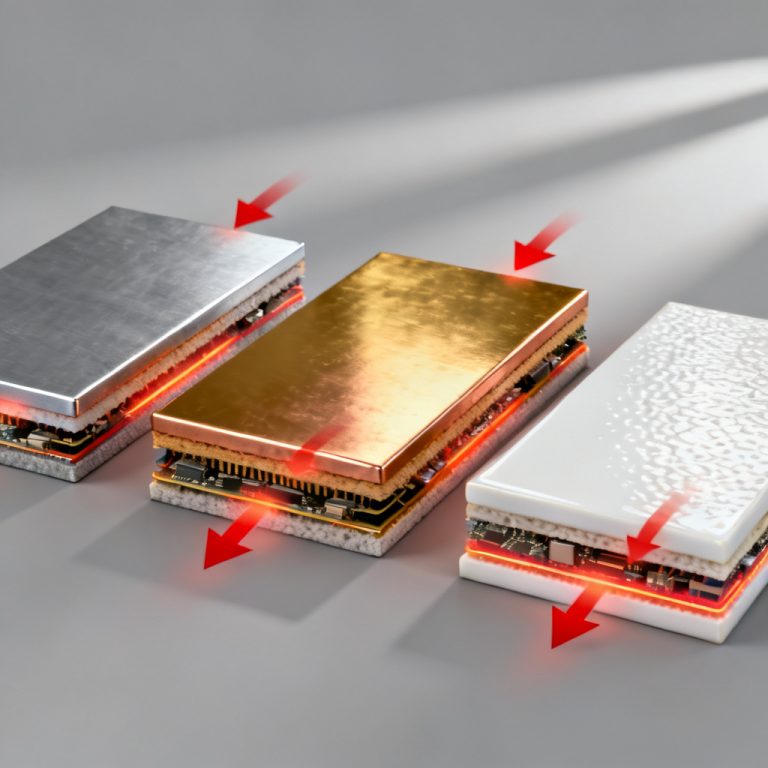
In modern electronics, the High Aspect Ratio PCB—combining thick substrates with extremely small drilled holes—is a critical enabler for miniaturization and high-density interconnects. This pillar content explores every facet of this complex technology, from fundamental definitions to advanced manufacturing, quality control, and application-specific considerations.
- What is a High Aspect Ratio PCB?
- Key Challenges in Manufacturing
- Advanced Manufacturing Techniques
- Material Considerations
- Design Guidelines
- Quality Control and Testing
- Applications
- Cost and Lead Time Considerations
- Future Trends
What is a High Aspect Ratio PCB?
Defining Aspect Ratio
The aspect ratio of a High Aspect Ratio PCB is the ratio of the board’s thickness to the diameter of the smallest drilled hole. For example, a 3.2mm thick board with a 0.2mm diameter hole has an aspect ratio of 16:1. While standard PCBs typically have aspect ratios of 5:1 to 8:1, high aspect ratio PCBs are generally defined as those exceeding 10:1, with advanced capabilities reaching 20:1 or even higher.
Why High Aspect Ratios Matter
High aspect ratios are essential for several reasons:
- Space Optimization: Thicker boards provide mechanical strength and thermal management, while small holes allow for dense routing and component placement.
- Signal Integrity: In high-frequency applications, shorter signal paths through small vias reduce inductance and crosstalk.
- Power Handling: Thicker copper layers in thick boards can carry higher currents, while small vias enable efficient power distribution.
- Reliability in Harsh Environments: Thick boards are more resistant to vibration and shock, making them ideal for aerospace, automotive, and industrial applications.
Key Challenges in Manufacturing High Aspect Ratio PCBs
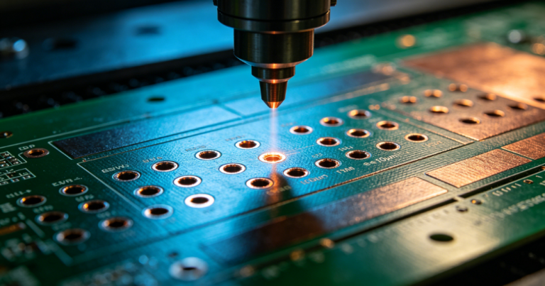
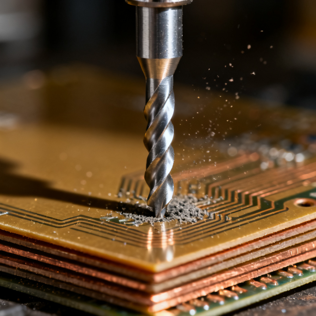
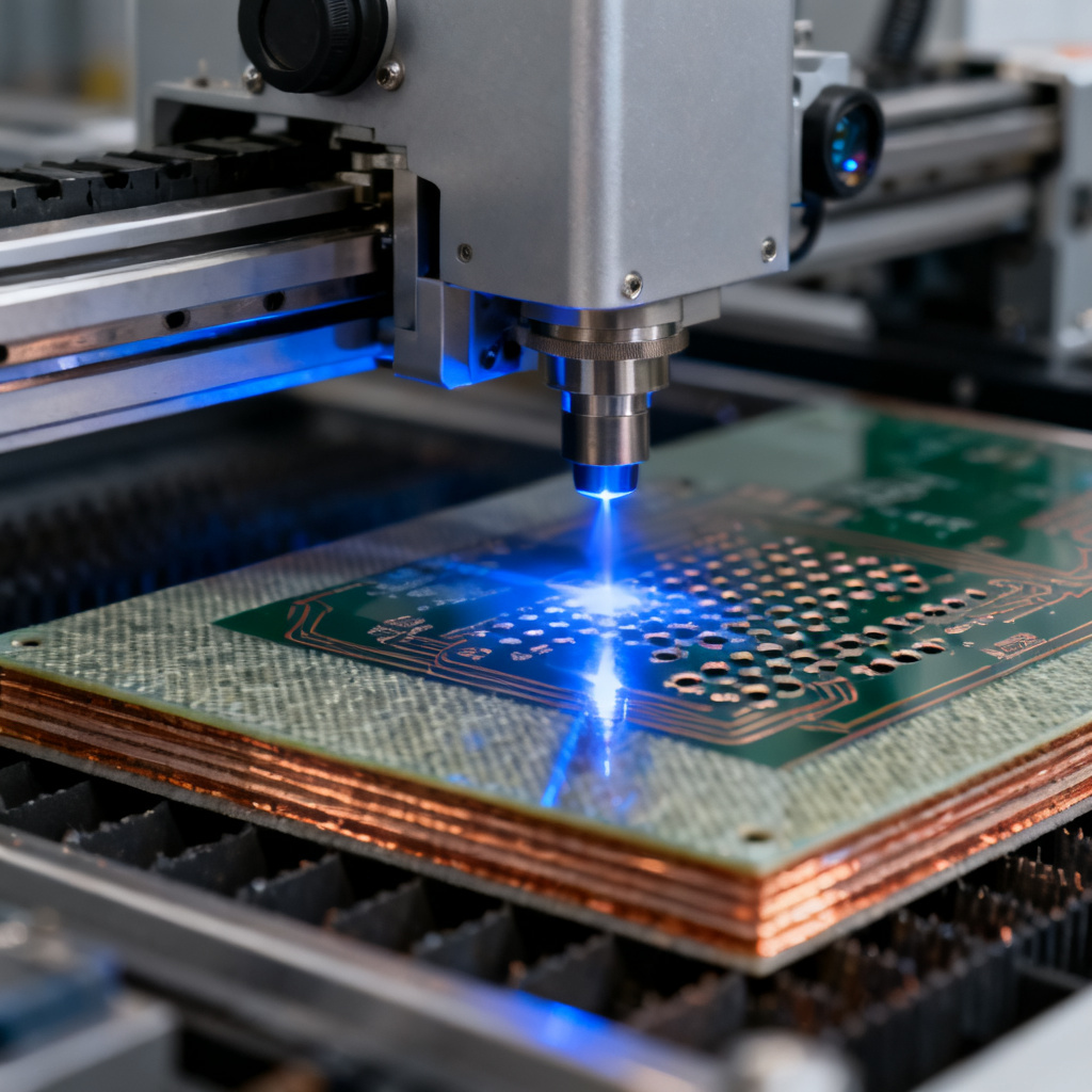
1. Drilling Precision and Tool Wear
Drilling small holes (e.g., 0.2mm diameter) through thick boards (e.g., 3.2mm) is extremely demanding. The drill bit must maintain perfect alignment and sharpness throughout the process. Key issues include:
- Tool Breakage: Thin drill bits (often 0.1–0.3mm in diameter) are prone to snapping under the stress of deep drilling.
- Heat Generation: Friction from deep drilling can melt resin and cause smearing, leading to poor hole wall quality.
- Chip Evacuation: Debris must be efficiently removed from deep, narrow holes to prevent clogging and bit damage.
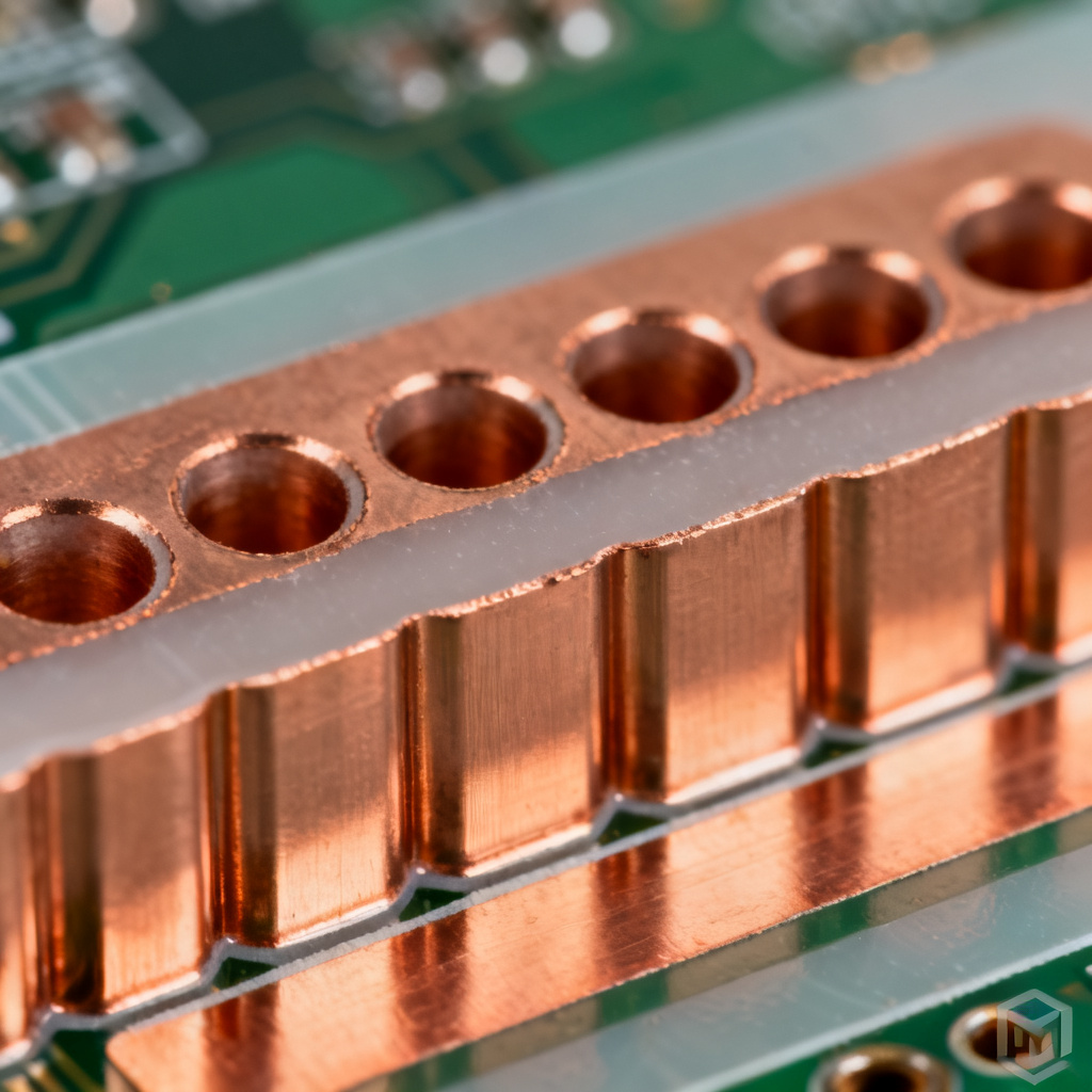
2. Plating Uniformity
Electroless and electrolytic copper plating must deposit a consistent thickness of copper inside deep, narrow holes. Challenges include:
- Throwing Power: The plating solution must reach the center of the hole, where current density is lowest. Poor throwing power results in thin copper at the hole’s midpoint, leading to reliability failures.
- Void Formation: Air bubbles or incomplete wetting can create voids in the copper layer, compromising electrical continuity.
- Uniformity Across the Panel: Variations in plating thickness across different areas of the board must be minimized.
3. Desmearing and Hole Wall Cleanliness
After drilling, the hole walls are covered with resin smear and glass fiber debris. In high aspect ratio holes, cleaning is difficult because:
- Limited Access: Chemical solutions and plasma gases struggle to penetrate deep, narrow holes.
- Resin Residue: Incomplete desmearing leaves a non-conductive layer that prevents proper copper adhesion.
- Glass Fiber Protrusions: Uneven etching can leave glass fibers exposed, causing reliability issues.
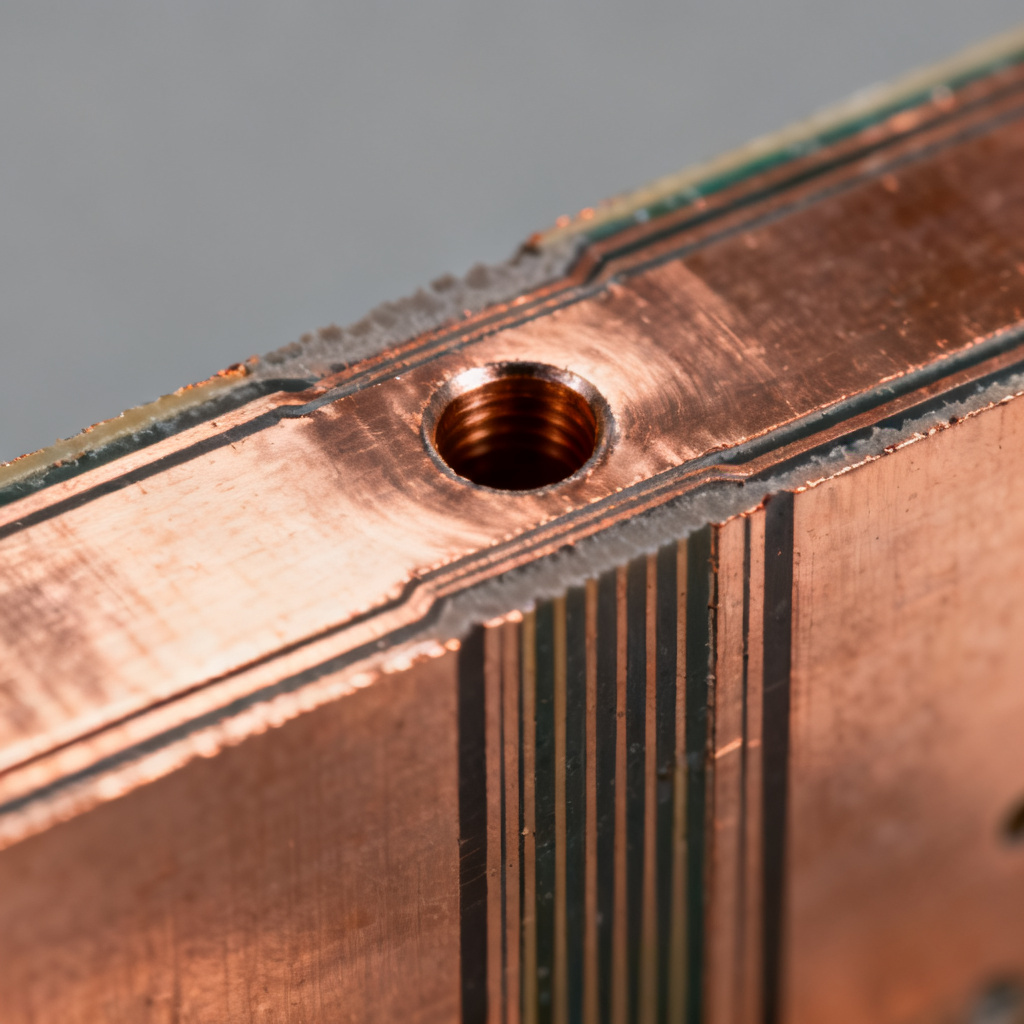
4. Registration and Layer-to-Layer Alignment
In multilayer PCBs, small holes must align perfectly with internal copper pads. For thick boards, thermal expansion and material shrinkage during lamination can cause misalignment. This is especially critical for high aspect ratio vias that connect multiple layers.
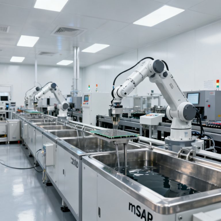
Advanced Manufacturing Techniques for High Aspect Ratio PCBs
Drilling Innovations
1. Specialized Drill Bits
- Carbide Micro-drills: Made from ultrafine grain tungsten carbide, these bits have enhanced wear resistance and sharpness.
- Coated Bits: Diamond-like carbon (DLC) or titanium nitride (TiN) coatings reduce friction and heat buildup.
- Optimized Geometry: Bits with special flute designs (e.g., parabolic flutes) improve chip evacuation in deep holes.
2. Controlled Drilling Parameters
- Step Drilling: For very high aspect ratios, holes are drilled in multiple passes (e.g., first a pilot hole, then final diameter) to reduce stress.
- Peck Drilling: The drill bit retracts periodically to clear chips and cool down.
- Optimized Feed and Speed: Lower feed rates and higher spindle speeds (up to 300,000 RPM) are used to minimize heat and tool wear.
3. Laser Drilling
For aspect ratios exceeding 20:1 or for very small holes (below 0.1mm), laser drilling is often preferred. CO2 and UV lasers can create clean, precise holes without mechanical stress. However, laser drilling is slower and more expensive than mechanical drilling.
Plating Solutions
1. High-Throw Electroless Copper
Advanced electroless copper baths with improved throwing power ensure uniform deposition in deep holes. Additives like wetting agents and accelerators help the solution penetrate narrow channels.
2. Pulse Plating
Instead of continuous DC current, pulse plating uses short bursts of high current followed by rest periods. This technique improves throwing power and grain structure, especially in high aspect ratio holes.
3. Horizontal Plating Lines
Vertical plating lines can struggle with uniformity in thick boards. Horizontal plating systems, where the board is conveyed through the bath, provide better solution flow and reduce the risk of voids.
4. Direct Metallization
Some manufacturers use conductive polymers or carbon-based coatings to replace the electroless copper step. These materials can penetrate deep holes more easily and reduce the number of process steps.
Desmearing and Cleaning
1. Plasma Desmearing
Oxygen and fluorine-based plasmas are highly effective at removing resin smear from deep holes. The plasma gas can penetrate narrow channels and chemically etch away organic residues without damaging glass fibers.
2. Wet Chemical Processes
- Sulfuric Acid Etch: Concentrated sulfuric acid removes resin smear but must be carefully controlled to avoid over-etching.
- Potassium Permanganate: This alkaline permanganate solution is used for desmearing in high aspect ratio holes, often in combination with plasma treatment.
3. Ultrasonic Cleaning
Ultrasonic agitation in cleaning baths helps dislodge debris and bubbles from deep holes, ensuring complete wetting before plating.
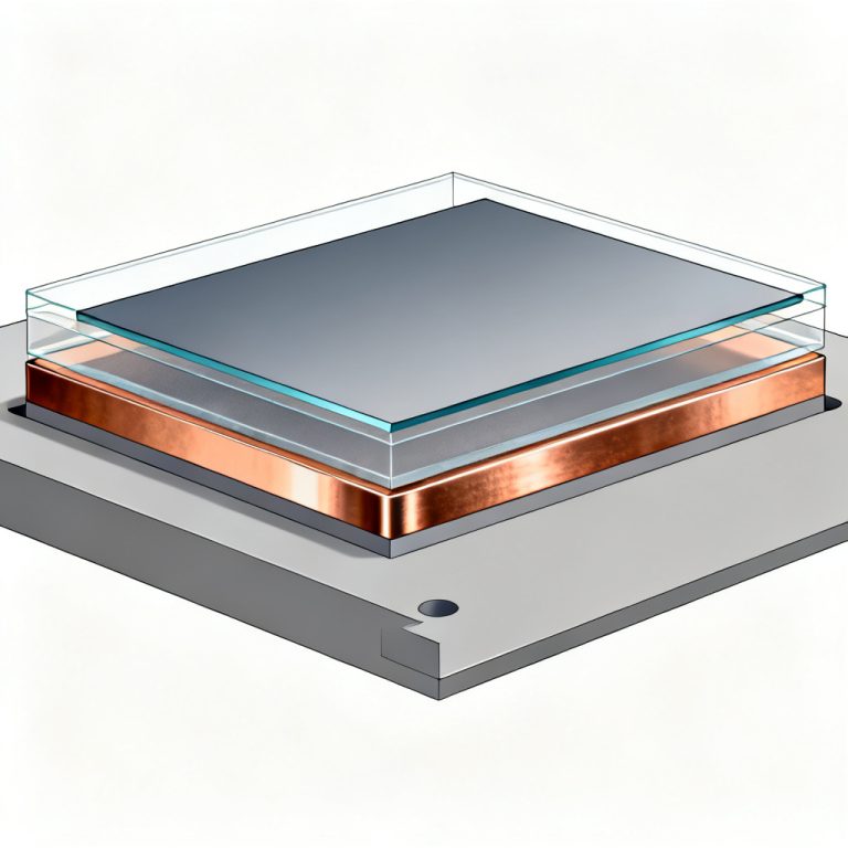
Material Considerations for High Aspect Ratio PCBs
Core Materials
- High-Tg Laminates: Materials with a high glass transition temperature (e.g., FR-4 with Tg > 170°C) are essential for thick boards to withstand thermal stress during drilling and soldering.
- Low CTE Materials: Low coefficient of thermal expansion (CTE) materials reduce the risk of misalignment and hole wall stress.
- Filled Resin Systems: Some advanced laminates use filled resins (e.g., with silica or glass microspheres) to improve dimensional stability and reduce resin smear.
Copper Foil
- Thick Copper: For power applications, thick copper foils (2 oz/ft² or more) are used. However, etching thick copper for small holes requires precise control to avoid undercut.
- Reverse Treat Foil: This type of foil has a rough surface on the inner side, improving adhesion to the laminate and reducing the risk of separation in deep holes.
Design Guidelines for High Aspect Ratio PCBs
Hole Size and Aspect Ratio Limits
| Capability Level | Aspect Ratio Range | Typical Application |
|---|---|---|
| Standard | Up to 10:1 | General electronics |
| Advanced | 10:1 to 20:1 | High-density interconnect |
| Extreme | Above 20:1 | Aerospace, defense, medical |
Via Types
- Through-Hole Vias: The most common type, drilled through the entire board. For high aspect ratios, consider using larger diameters if possible.
- Blind and Buried Vias: These vias connect only specific layers, reducing the thickness that must be drilled. Sequential lamination is required.
- Microvias: With diameters of 0.1mm or less, microvias are typically laser-drilled and have aspect ratios of 1:1 or lower.
Pad and Annular Ring Design
- Minimum Annular Ring: For high aspect ratio holes, a larger annular ring (e.g., 0.1mm or more) is recommended to account for drilling tolerance and misalignment.
- Teardrop Pads: Using teardrop-shaped pads at the connection points reduces stress concentration and improves reliability.
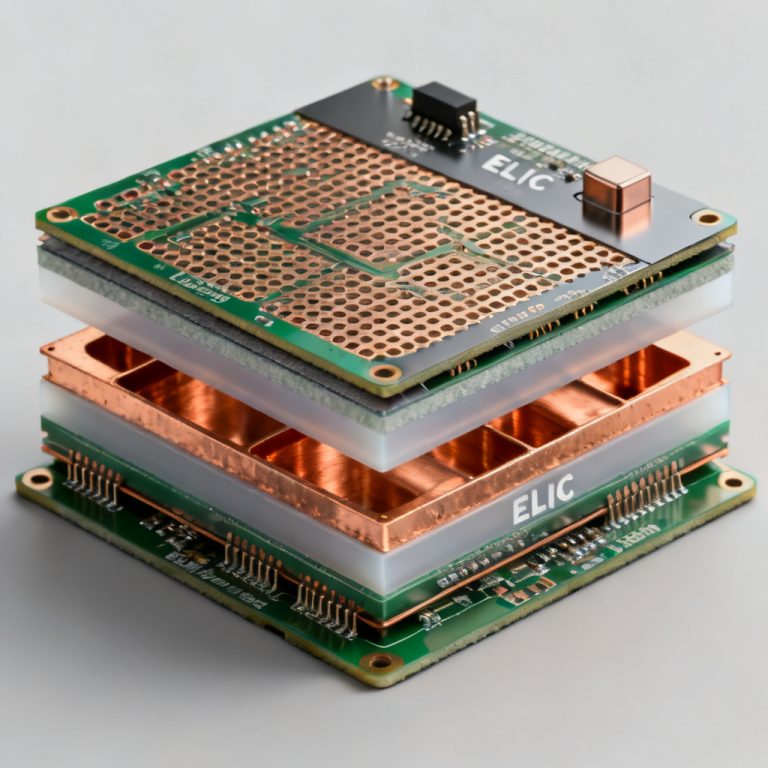
Stackup Considerations
- Symmetrical Stackup: To prevent warpage, the board should be symmetrical in terms of copper distribution and layer thickness.
- Core vs. Prepreg: Thick cores (e.g., 1.0mm or more) are preferred for high aspect ratio boards, as they provide better dimensional stability than multiple prepreg layers.
Quality Control and Testing
Microsection Analysis
Microsectioning is the primary method for evaluating hole quality. Cross-sections of the board are examined under a microscope to check:
- Copper Thickness: Measured at the top, middle, and bottom of the hole. Minimum acceptable thickness is typically 20–25 microns.
- Void Detection: Any voids in the copper layer are noted and measured.
- Hole Wall Roughness: Excessive roughness can indicate drilling or plating issues.
Electrical Testing
- Continuity Testing: Ensures that all vias are electrically connected.
- Resistance Measurement: High aspect ratio vias can have higher resistance due to thinner copper in the center. Resistance should be within specified limits.
- Impedance Testing: For high-frequency applications, impedance must be controlled.
Thermal Stress Testing
- Solder Float Test: The board is floated on molten solder (288°C for 10 seconds) to simulate soldering conditions. After testing, microsections are checked for cracks or delamination.
- Thermal Cycling: Boards are subjected to multiple cycles of extreme temperatures (e.g., -40°C to +125°C) to evaluate reliability.
X-Ray Inspection
X-ray imaging is used to verify alignment between drilled holes and internal pads, especially in multilayer boards. This is critical for high aspect ratio boards where misalignment can lead to open circuits.
Applications of High Aspect Ratio PCBs
Aerospace and Defense
- Avionics: Thick boards with high aspect ratio vias are used in flight control systems, radar, and communication equipment.
- Satellites: Space-grade PCBs require high reliability under extreme thermal and radiation conditions.
Automotive Electronics
- Engine Control Units (ECUs): High aspect ratio PCBs handle high currents and vibrations in engine compartments.
- Advanced Driver-Assistance Systems (ADAS): Dense routing in thick boards supports sensor fusion and processing.
Industrial and Medical
- Power Inverters: Thick copper boards with high aspect ratio vias manage high currents in industrial drives.
- Medical Imaging: MRI and CT scanners use high aspect ratio PCBs for signal integrity and reliability.
Telecommunications
- 5G Infrastructure: Base stations and antennas require thick boards with controlled impedance and high aspect ratio vias for signal routing.
- Data Centers: High-speed switches and routers benefit from dense, reliable interconnects.
Cost and Lead Time Considerations
Factors Affecting Cost
- Aspect Ratio: Higher aspect ratios require specialized equipment and more process steps, increasing cost.
- Board Thickness: Thicker boards consume more material and require longer processing times.
- Hole Density: Boards with many small holes are more expensive to drill and plate.
- Material Selection: High-Tg or low-CTE laminates cost more than standard FR-4.
Lead Time
| Aspect Ratio Range | Typical Lead Time | Process Complexity |
|---|---|---|
| Up to 10:1 | 5–10 business days | Standard |
| 10:1 to 16:1 | 10–15 business days | Moderate |
| Above 16:1 | 15–25 business days | High |
Future Trends in High Aspect Ratio PCB Technology
1. Additive Manufacturing
3D printing of PCBs using conductive inks and insulating polymers could enable aspect ratios beyond current limits, with holes as small as 0.05mm.
2. Advanced Laser Systems
Femtosecond lasers offer ultra-precise drilling without heat-affected zones, making them ideal for extreme aspect ratios.
3. AI-Controlled Drilling
Machine learning algorithms can optimize drilling parameters in real-time, reducing tool wear and improving hole quality.
4. New Materials
Graphene-based composites and ceramic-filled laminates may offer better thermal and mechanical properties for high aspect ratio boards.
Comparison: Standard PCB vs. High Aspect Ratio PCB
| Parameter | Standard PCB | High Aspect Ratio PCB |
|---|---|---|
| Aspect Ratio | 5:1 to 8:1 | 10:1 to 20:1+ |
| Minimum Hole Diameter | 0.3mm | 0.1mm – 0.2mm |
| Board Thickness | Up to 1.6mm | 2.0mm – 6.0mm |
| Plating Uniformity | Easy to achieve | Requires advanced processes |
| Cost | Lower | Higher (due to complexity) |
| Lead Time | 5–7 days | 10–25 days |
Industry Terminology Explained
- Aspect Ratio: The ratio of board thickness to smallest hole diameter.
- Throwing Power: The ability of a plating solution to deposit metal uniformly in deep, narrow holes.
- Desmearing: The process of removing resin residue from drilled hole walls to ensure proper copper adhesion.
- Microvia: A very small via (typically <0.15mm diameter) used in high-density interconnect designs.
- High-Tg Laminate: A material with a high glass transition temperature, suitable for high-temperature applications.
Frequently Asked Questions (FAQ)
What is the maximum aspect ratio achievable for a High Aspect Ratio PCB?
With advanced drilling and plating technologies, aspect ratios up to 20:1 are commercially viable, while extreme cases can exceed 20:1 using laser drilling and specialized processes.
How does a High Aspect Ratio PCB improve signal integrity?
By enabling shorter signal paths through small vias in thick boards, high aspect ratio PCBs reduce inductance and crosstalk, which is critical for high-frequency digital and RF designs.
What are the main challenges in plating High Aspect Ratio PCBs?
The primary challenges include achieving uniform copper deposition in deep, narrow holes (throwing power), preventing voids, and maintaining consistent thickness across the entire panel.
Which industries most commonly use High Aspect Ratio PCBs?
Aerospace, defense, automotive (especially ADAS and ECUs), medical imaging, and telecommunications (5G infrastructure) frequently rely on high aspect ratio PCBs for their demanding performance and reliability requirements.
Can standard FR-4 be used for High Aspect Ratio PCBs?
Standard FR-4 is generally not recommended for high aspect ratio PCBs due to its higher CTE and lower Tg. High-Tg laminates or low-CTE materials are preferred to ensure reliability during drilling, plating, and thermal cycling.