This comprehensive DDR4/DDR5 PCB Design Guide covers timing constraints and signal integrity techniques for high-speed memory interfaces, essential for engineers and PCB manufacturers.
Designing PCBs for DDR4 and DDR5 memory interfaces is a high-stakes endeavor. As data rates soar from 3200 MT/s (DDR4) to 6400 MT/s (DDR5) and beyond, the margin for error shrinks dramatically. This guide consolidates the most authoritative insights from JEDEC standards, leading EDA tool vendors, and industry white papers. We cover everything from topology selection and impedance matching to timing closure and power integrity. Whether you are a seasoned engineer or a procurement specialist evaluating PCB manufacturers, this pillar content provides the technical depth needed to ensure first-pass success and reliable high-speed operation.
1. Understanding DDR4 vs. DDR5: Key Architectural Differences for Your DDR4/DDR5 PCB Design
Before diving into layout rules, it is crucial to grasp the fundamental differences between DDR4 and DDR5 that impact DDR4/DDR5 PCB design.
- Data Rate and Bandwidth: DDR4 typically ranges from 1600 to 3200 MT/s. DDR5 starts at 4800 MT/s and scales to 6400 MT/s and beyond. This directly increases signal integrity challenges.
- On-Die Termination (ODT) and Dynamic ODT: DDR5 introduces more granular ODT control. While DDR4 has fixed ODT values per rank, DDR5 allows dynamic ODT changes during read/write operations to better match impedance and reduce reflections. This requires careful simulation of ODT states.
- Voltage Levels: DDR4 uses VDD of 1.2V. DDR5 drops to 1.1V, reducing power but also shrinking noise margins. Signal integrity becomes more critical.
- DIMM vs. Soldered Memory: For DDR5, the memory controller is often on the CPU (for desktop) or integrated into the SoC (for embedded). However, for B2B custom boards, soldered-down (discrete) DDR5 is common. This changes routing constraints (no DIMM connector parasitics).
- Training and Calibration: DDR5 has more extensive training sequences (e.g., DQ/DQS training, CA training, read/write leveling) that rely on precise PCB timing. The PCB must support these sequences without introducing skew.
Key Takeaway: DDR5 is not just a faster DDR4. It requires tighter impedance control, lower crosstalk, and more sophisticated power delivery networks (PDNs).
2. Critical Timing Constraints for DDR4/DDR5 PCB Design
Timing is the backbone of memory interface design. The following parameters must be understood and met.
2.1 Clock Timing (CK, CK#)
- Differential Clocking: Both DDR4 and DDR5 use a differential clock (CK_t, CK_c). The clock must have a 50% duty cycle and low jitter.
- Skew: The intra-pair skew (between CK_t and CK_c) must be < ±5 ps (recommended < ±2 ps for DDR5). The inter-pair skew (between different clock pairs) must be tightly controlled.
- Length Matching: Clock traces must be matched to within 10 mils for DDR4, and within 5 mils for DDR5, relative to the memory controller and each DIMM/device.
2.2 Data Timing (DQ, DQS, DM)
- DQS as a Strobe: DQS is a bidirectional strobe used for data capture. DQ signals must be matched to their corresponding DQS within a tight window.
- Data Skew: For DDR4, DQ to DQS skew must be < ±10 ps (typical). For DDR5, it must be < ±5 ps due to the higher data rate.
- Write Leveling: For DDR5, write leveling is mandatory to compensate for clock-to-strobe skew across multiple devices. This requires that DQS and CK are matched within a few ps.
- Read Timing: The controller uses DQS to capture DQ during reads. Read timing is affected by flight time and process variations. Ensure that DQS and DQ have matched propagation delays.
2.3 Address/Command Timing (CA, CS, CKE, ODT)
- CA Bus: DDR4 uses a single 14-bit CA bus. DDR5 splits it into two 7-bit CA buses (CA_A and CA_B) for each channel. This reduces loading but requires careful skew control between CA_A and CA_B.
- Setup and Hold Times: CA signals must meet the setup and hold times relative to the rising edge of CK. For DDR5, the setup/hold window is approximately 0.2 UI (unit interval), which is < 30 ps at 6400 MT/s.
- Length Matching: CA lines should be length-matched to within 20 mils for DDR4, and within 10 mils for DDR5. They must also be matched to the clock.
2.4 Timing Budget and Derating
- Jitter and Noise: Include jitter from the PLL, crosstalk, and power supply noise in your timing budget. Use derating factors from the JEDEC datasheet (e.g., for voltage and temperature variations).
- Flight Time: Account for PCB trace delay (approximately 140-180 ps/inch for microstrip, 160-200 ps/inch for stripline). Use simulation tools like HyperLynx or Sigrity to verify.
Practical Rule: For DDR5, a common rule of thumb is: DQ to DQS within ±2 ps, CA to CK within ±5 ps, and clock to clock within ±2 ps. Always simulate worst-case corners.
3. Signal Integrity (SI) Principles and Techniques for Your DDR4/DDR5 PCB Design
Signal integrity is about preserving the quality of the digital signal from driver to receiver.
3.1 Impedance Control
- Target Impedance: DDR4: 50Ω single-ended (for DQ, CA), 100Ω differential (for DQS, CK). DDR5: 40Ω single-ended (due to lower voltage and higher speed) and 80Ω differential. Confirm with your memory vendor.
- Stackup Design: Use a 4-layer or 6-layer stackup for DDR4, and 6-layer or 8-layer for DDR5. Signal layers should be adjacent to a solid ground plane. Use controlled dielectric materials (e.g., FR4 with low loss tangent for DDR5).
- Trace Width and Spacing: Calculate trace width for target impedance using a field solver (e.g., Polar). For typical 50Ω microstrip on 0.062” FR4, width is ~8-10 mils. For 40Ω, width may be ~12-15 mils.
3.2 Termination and On-Die Termination (ODT)
- ODT Values: DDR4: 40Ω, 60Ω, 120Ω (programmable). DDR5: 34Ω, 48Ω, 60Ω. ODT is placed near the receiver to absorb reflections.
- Dynamic ODT (DDR5): The ODT value can change during a burst. For example, during a write, the DRAM uses a lower ODT (e.g., 34Ω) to match the driver impedance. This must be simulated.
- VTT Termination: For CA and control signals, use a VTT termination (VDD/2) with a resistor to the termination voltage. Place termination resistors close to the last device.
3.3 Crosstalk Mitigation
- Spacing: Keep DQ lines spaced at least 3x the trace width (3W rule) to reduce crosstalk. For DDR5, use 4W or 5W.
- Guard Traces: In dense areas, route ground guard traces between sensitive signals (e.g., between DQ and CA). Ensure the guard trace is stitched to ground with vias.
- Layer Assignment: Place high-speed signals (CK, DQS) on inner layers (stripline) to reduce EMI and crosstalk. Use microstrip for less critical signals if needed.
3.4 Reflections and Ringing
- Length of Stubs: Minimize stub lengths (e.g., from vias). For DDR5, vias with stub lengths > 10 mils can cause significant reflections. Use back-drilling or blind vias.
- Series Termination: For point-to-point signals (e.g., CA in some topologies), add a series resistor (22-33Ω) near the driver to dampen ringing.
3.5 Power Integrity (PDN)
- Decoupling Capacitors: Use a mix of bulk (10-100 µF), ceramic (0.1-1 µF), and high-frequency (10-100 pF) capacitors. Place them as close as possible to the memory power pins.
- Power Plane: Use a solid VDD plane (1.2V for DDR4, 1.1V for DDR5) with low inductance. The plane should be adjacent to the ground plane to form a low-ESL capacitor.
- Target Impedance: For DDR5, the target PDN impedance is < 10 mΩ up to 100 MHz. This requires careful capacitor selection and placement.
4. PCB Layout and Routing Guidelines for DDR4/DDR5 PCB Design
4.1 Topology Selection
- DDR4: Common topologies are T-topology (fly-by for address/command, T for data) or fly-by for all signals. Fly-by is preferred for high-speed to reduce stub effects.
- DDR5: Fly-by topology is mandatory for CA and control signals. Data groups (DQ/DQS) use point-to-point routing between the controller and each device (or DIMM). This eliminates the need for T-branches.
4.2 Length Matching Rules
- Data Group (DQ0-DQ7, DQS0, DM0): Match all signals in the same byte lane to within ±10 mils (DDR4) or ±5 mils (DDR5). Match DQS to CK within ±20 mils (DDR4) or ±10 mils (DDR5).
- Address/Command Group: Match CA signals to CK within ±25 mils (DDR4) or ±15 mils (DDR5).
- Clock Group: Match CK pairs to each other within ±10 mils.
- Inter-Group Matching: For DDR5, match all CA groups to each other within ±25 mils. For DDR4, match all data groups to the clock within ±100 mils.
4.3 Via and Layer Transitions
- Via Count: Minimize via count per net. Each via adds ~1-2 ps delay and impedance discontinuity. For DDR5, limit to 2 vias per net.
- Via Stub: Use back-drilling to remove via stubs for signals above 3200 MT/s. Alternatively, use microvias (HDI) for soldered-down memory.
- Layer Change: When changing layers, place a ground via adjacent to the signal via to maintain return current path.
4.4 Routing for Differential Pairs
- Match Length: Match the two traces of a differential pair to within ±2 mils.
- Spacing: Keep intra-pair spacing constant (e.g., 5-6 mils) to maintain differential impedance.
- Avoid 90° Bends: Use 45° or arc bends to minimize impedance change.
4.5 Power and Ground Routing
- Solid Planes: Use a dedicated ground plane adjacent to each signal layer. For DDR5, use a split power plane (VDD1.1V, VPP2.5V, VDDQ1.1V) with proper isolation.
- Bypass Capacitors: Place capacitors on the same side of the board as the memory, within 100 mils of the power pin.
5. Simulation and Verification for Your DDR4/DDR5 PCB Design
5.1 Pre-Layout Simulation
- IBIS Models: Obtain IBIS models from the memory vendor (e.g., Micron, Samsung, SK Hynix) and the controller vendor.
- Topology Simulation: Simulate the topology (fly-by, point-to-point) to determine optimal ODT values and termination.
- Timing Budget: Use a spreadsheet to calculate worst-case timing margins including jitter, skew, and derating.
5.2 Post-Layout Simulation
- Extraction: Extract parasitic RLC from the PCB layout using a field solver (e.g., Ansys Q3D, Cadence Sigrity).
- Time-Domain Simulation: Run transient simulations to check for overshoot, undershoot, and eye diagram closure. For DDR5, the eye opening at the receiver must be > 0.5 UI.
- Crosstalk Analysis: Use a coupled-line simulation to verify that crosstalk is below 5% of the signal amplitude.
5.3 Physical Validation
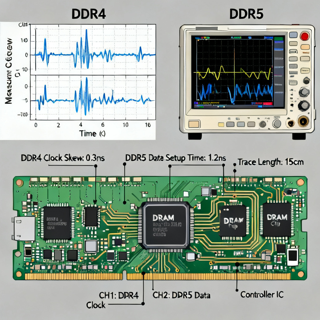
- TDR (Time-Domain Reflectometry): Measure impedance of critical traces (CK, DQS) using a TDR. Target impedance should be within ±10% of the target.
- Eye Diagram Measurement: Use a high-speed oscilloscope to measure eye diagrams at the memory device. Ensure the eye is open with sufficient margin.
6. B2B Manufacturing Considerations for DDR4/DDR5 PCB Design
6.1 PCB Material Selection
- For DDR4: Standard FR4 (e.g., ISOLA 370HR) is often sufficient for up to 3200 MT/s. Use low-loss FR4 if routing is long (>6 inches).
- For DDR5: Use high-speed laminates (e.g., Megtron 6, Rogers 4350B) to minimize dielectric loss. The dissipation factor (Df) should be < 0.01 at 1 GHz.
6.2 Impedance Tolerance
- Standard: Most PCB manufacturers offer ±10% impedance tolerance. For DDR5, request ±5% tolerance and controlled etching.
- Copper Roughness: Specify low-profile copper (e.g., RTF or VLP) to reduce skin effect losses at high frequencies.
6.3 Layer Stackup
- DDR4 (4-layer): Signal-Ground-Power-Signal. Ensure ground plane is solid under all memory signals.
- DDR5 (6-layer): Signal-Ground-Signal-Power-Ground-Signal. Use two ground planes for improved isolation.
- Thickness: Keep the total board thickness between 0.062” and 0.093” for standard manufacturing.
6.4 Testing and Quality Assurance
- Flying Probe Test: Test all memory nets for shorts and opens.
- Impedance Coupon: Include a test coupon on the panel for impedance verification.
- X-Ray Inspection: For BGA packages (e.g., FBGA for DDR5), use X-ray to verify solder joint quality.
Comparison: DDR4 vs. DDR5 PCB Design
| Parameter | DDR4 PCB Design | DDR5 PCB Design |
|---|---|---|
| Target Single-Ended Impedance | 50Ω | 40Ω |
| Target Differential Impedance | 100Ω | 80Ω |
| Data Rate | 1600-3200 MT/s | 4800-6400 MT/s |
| Voltage (VDD) | 1.2V | 1.1V |
| ODT Values | 40Ω, 60Ω, 120Ω | 34Ω, 48Ω, 60Ω |
| Topology | T-topology or fly-by | Fly-by (CA), point-to-point (DQ) |
| Recommended Stackup | 4-layer or 6-layer | 6-layer or 8-layer |
| Material | Standard FR4 | High-speed laminate (e.g., Megtron 6) |
Glossary of Key Terms for DDR4/DDR5 PCB Design

- Signal Integrity (SI): The quality of an electrical signal as it travels from driver to receiver, affected by impedance, crosstalk, and reflections.
- On-Die Termination (ODT): Termination resistors integrated into the DRAM die to match impedance and reduce reflections.
- Fly-By Topology: A routing method where signals daisy-chain through devices, reducing stub effects.
- Power Delivery Network (PDN): The system of power planes, vias, and capacitors that supply stable voltage to the memory.
- JEDEC: The standards body that defines DDR memory specifications (e.g., JESD79-4 for DDR4, JESD79-5 for DDR5).
Frequently Asked Questions (FAQ) about DDR4/DDR5 PCB Design
What is the most critical aspect of a DDR4/DDR5 PCB design guide?
The most critical aspect is managing timing and signal integrity, including impedance control, length matching, and crosstalk mitigation, as outlined in this DDR4/DDR5 PCB Design Guide.
How do I choose between DDR4 and DDR5 for my PCB design?
Consider your data rate requirements, power budget, and cost. DDR5 offers higher bandwidth and lower voltage but requires more advanced PCB materials and tighter design rules, as detailed in this DDR4/DDR5 PCB Design Guide.
What impedance should I target for DDR5 traces?
For DDR5, target 40Ω single-ended and 80Ω differential, which is a key difference from DDR4 and is covered in this DDR4/DDR5 PCB Design Guide.
Why is fly-by topology recommended for DDR5?
Fly-by topology reduces stub effects and improves signal integrity at high data rates, a recommendation emphasized in this DDR4/DDR5 PCB Design Guide.
What materials are best for DDR5 PCBs?
High-speed laminates like Megtron 6 or Rogers 4350B are recommended for DDR5 to minimize dielectric loss, as discussed in this DDR4/DDR5 PCB Design Guide.
Conclusion
Designing a PCB for DDR4 or DDR5 memory requires a holistic approach that balances timing, signal integrity, power integrity, and manufacturing constraints. By following the guidelines in this DDR4/DDR5 PCB Design Guide—from topology selection and impedance control to simulation and material choice—you can achieve first-pass success. Remember that DDR5 pushes the boundaries of traditional PCB design; invest in simulation tools and partner with a PCB manufacturer experienced in high-speed memory interfaces. For B2B buyers, specifying these requirements in your RFQ ensures that your supplier delivers a board that meets the rigorous demands of modern memory systems.
External References: JEDEC DDR4/DDR5 Standards (JESD79-4, JESD79-5), Micron DDR5 Design Guide, Altium DDR5 Routing Guidelines, Cadence Signal Integrity White Papers.