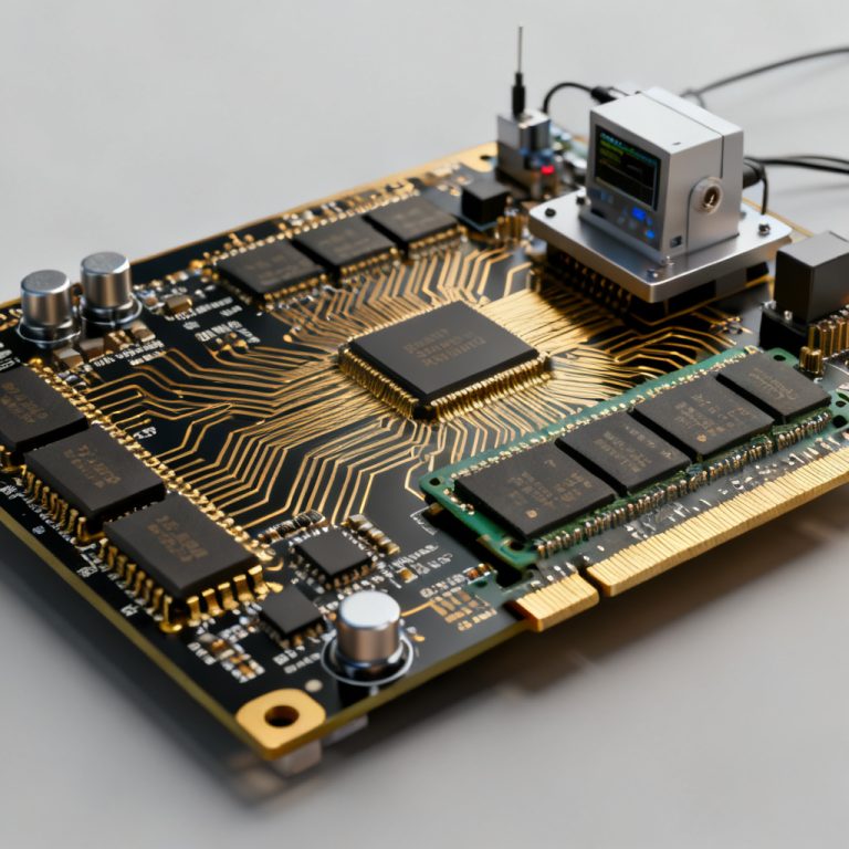
In the world of high-speed digital systems, the high-speed backplane PCB is the nervous system. It connects line cards, switch fabrics, and power modules, handling data rates that now routinely exceed 25 Gbps per lane. At these speeds, two critical challenges dominate the design and manufacturing landscape: Press-Fit connector reliability and Via Stub removal. Ignoring either can lead to signal degradation, intermittent failures, and costly redesigns.
This Pillar Content is your definitive guide. We will dissect the engineering principles, design rules, and manufacturing best practices for creating high-speed backplane PCBs that deliver impeccable signal integrity (SI) and mechanical robustness.
What Is a High-Speed Backplane PCB?
A high-speed backplane PCB is a passive or active printed circuit board that acts as a communication backbone. Unlike standard PCBs, backplanes are characterized by:
- High Layer Counts: Typically 20 to 40+ layers to route hundreds or thousands of differential pairs.
- Large Form Factors: Often exceeding 18” x 24”, requiring careful stack-up management to prevent warpage.
- High-Speed SerDes Lanes: Data rates from 10 Gbps (NRZ) up to 112 Gbps (PAM-4) are common.
- Dense Connector Arrays: Thousands of press-fit pins for mezzanine or card-edge connectors.
The performance of a high-speed backplane PCB is dictated by its ability to maintain a consistent impedance (e.g., 85Ω or 100Ω differential) and minimize losses (insertion loss, return loss, crosstalk).
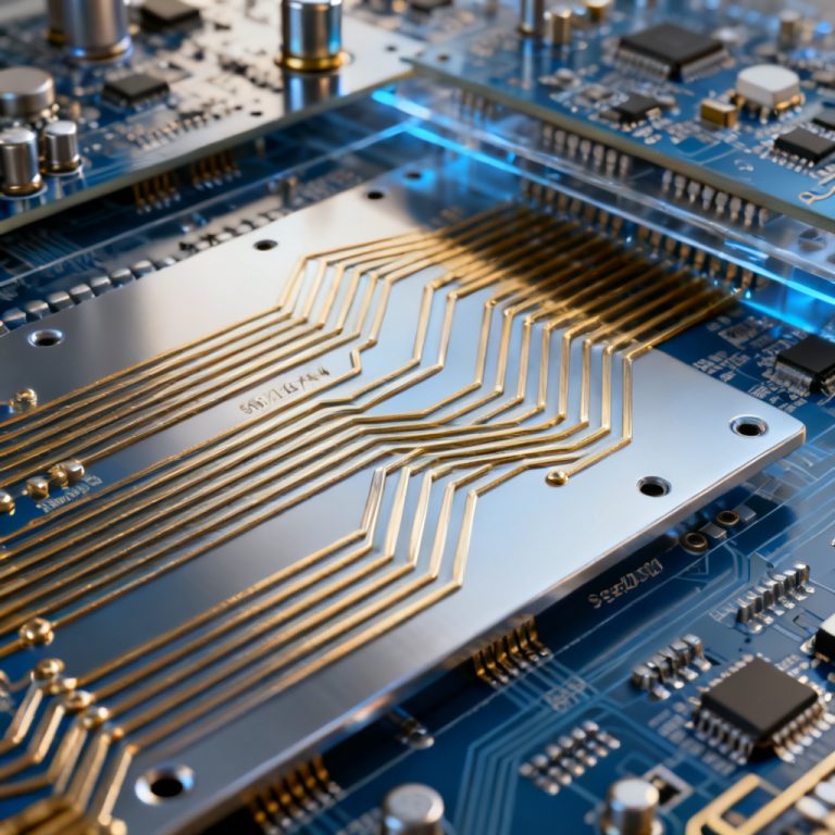
Press-Fit Technology for High-Speed Backplane PCBs
Press-fit technology is the industry standard for high-speed backplane PCB connectors because it eliminates the need for soldering, reducing thermal stress and enabling easier field repairs. However, it introduces unique design constraints.
The Press-Fit Principle
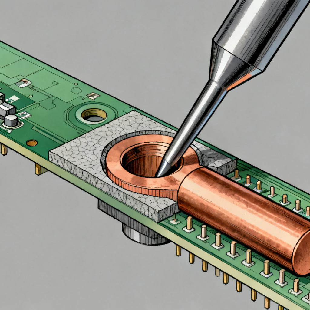
A press-fit pin (compliant pin) is designed to be slightly larger than the plated through-hole (PTH) diameter. When pressed in, the pin’s flexible “eye of the needle” or “action pin” deforms, creating a gas-tight, cold-weld joint between the pin and the copper barrel.
Key Requirements for a Reliable Press-Fit Joint:
- Hole Size Tolerance: The PTH diameter must be tightly controlled. A typical spec is ±0.05mm (2 mils) for a 0.6mm finished hole. Too large, and the pin loses retention force; too small, and the pin may be damaged or the board may crack.
- Plating Thickness: Minimum 25 microns (1 mil) of copper in the barrel is standard. Thicker plating provides better mechanical grip but increases stress.
- Annular Ring: The copper pad surrounding the hole must be wide enough to prevent breakout during insertion. A minimum of 0.2mm (8 mils) is recommended for internal and external layers.
- Board Thickness: Press-fit pins are designed for a specific board thickness range (e.g., 1.6mm to 3.2mm). Too thin, and the pin protrudes; too thick, and it may not fully seat.
The Hidden Danger: Stress-Induced Cracks
During press-fit insertion, the high-speed backplane PCB experiences significant mechanical stress. This can cause:
- Barrel Cracking: Micro-cracks in the copper plating, especially in the mid-board region, leading to intermittent opens.
- Pad Lifting: The copper pad separates from the laminate due to excessive Z-axis stress.
- Laminate Delamination: High stress near the hole can cause the resin to separate from the glass weave.
Mitigation Strategies:
- Use high-Tg (170°C+) and low-CTE (Coefficient of Thermal Expansion) laminates like Isola 370HR or Megtron 6.
- Employ a back-drilling process (discussed later) to remove unused stubs, which also reduces mechanical stress on the barrel.
- Specify a controlled insertion force during assembly. The press-fit tool must be calibrated to avoid over-pressing.
Electrical Performance of Press-Fit Connections
At high frequencies, the press-fit pin acts as a small impedance discontinuity. The transition from the PCB trace to the connector pin must be optimized:
- Anti-Pad Design: The clearance hole (anti-pad) around the via on power/ground planes must be large enough to maintain 100Ω differential impedance. A typical anti-pad diameter is 0.6mm to 1.0mm larger than the via diameter.
- Stub Length: The portion of the via that extends beyond the signal layer (the stub) is a primary cause of resonance and signal reflection. This leads directly to our next critical topic.
Via Stub Removal in High-Speed Backplane PCBs
A via stub is the unused portion of a plated through-hole that extends from the lowest signal layer to the bottom of the board. At low frequencies, this stub is invisible. But at 10+ Gbps, it acts as a transmission line stub, causing resonant notches in the insertion loss (S21) and increasing return loss (S11).
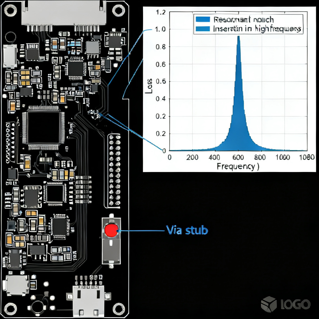
Why Stubs Are Deadly
Imagine a 1/4-wave resonant stub. At the resonant frequency, the stub reflects the signal back to the source, effectively shorting it out. The formula for the first resonant frequency is:
f_res = c / (4 × L_stub × √ε_r)
Where:
- c = speed of light
- L_stub = stub length
- ε_r = dielectric constant of the PCB material
Example: A 50-mil stub in FR4 (Er~4.2) resonates at approximately 7.5 GHz. For a 25 Gbps signal (fundamental frequency ~12.5 GHz), this stub will cause severe signal degradation.
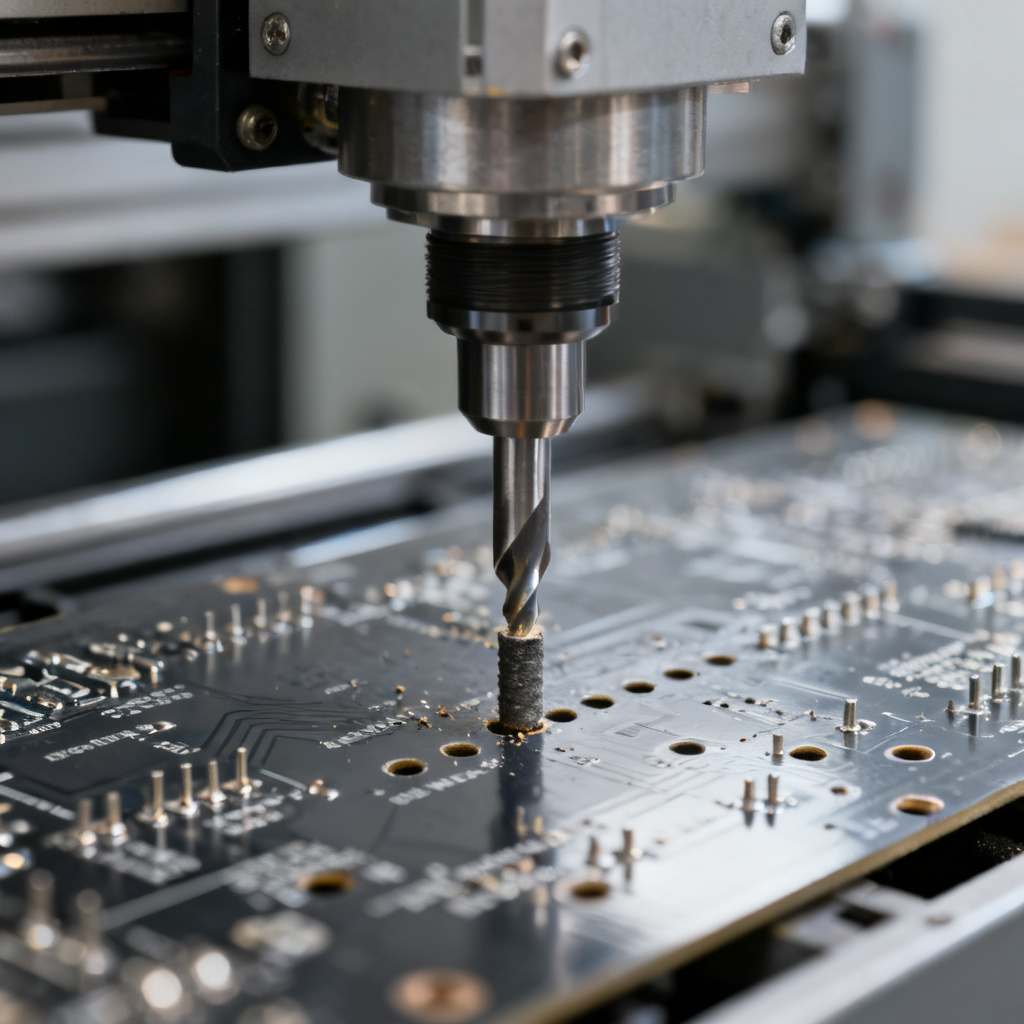
The Solution: Back-Drilling (Controlled Depth Drilling)
Back-drilling is a post-lamination process where a larger drill bit (e.g., 0.8mm to 1.0mm) is used to remove the copper barrel of the unused stub from the bottom side of the board. The goal is to leave only the required signal path.
The Back-Drilling Process:
- Standard Drilling & Plating: The via is drilled and plated as usual.
- Back-Drill Operation: A CNC machine drills from the bottom side of the board, stopping precisely at a depth just below the lowest signal layer.
- Depth Control: The critical parameter is the back-drill depth tolerance. Typical specs require the drill to stop within 0.2mm (8 mils) of the target layer. Too deep, and you cut into the signal trace; too shallow, and you leave a residual stub.
- Cleaning: The back-drilled hole is cleaned to remove debris and copper whiskers.
Important Note: Back-drilling removes the copper from the barrel, but the glass weave and resin remain. This is acceptable because the remaining material is non-conductive.
When Is Back-Drilling Required?
- Data Rates > 10 Gbps: Mandatory for NRZ signaling at 10 Gbps and above.
- Data Rates > 25 Gbps: Absolutely critical for 25 Gbps NRZ or 56 Gbps PAM-4.
- Long Stubs (> 30 mils): Even at lower speeds, long stubs can cause issues.
- High-Density Designs: When many vias are present, stub resonance can couple between channels.
Advanced Techniques: Stub Removal vs. Stub Reduction
- Traditional Back-Drilling: Removes the stub from the bottom side. Works well for signals routed on top layers.
- Sequential Lamination (Buried Vias): Eliminates stubs entirely by using microvias and buried vias. This is the most expensive but highest-performance solution.
- Reverse Back-Drilling: Drilling from the top side to remove stubs for signals routed on bottom layers. This is less common due to component clearance issues.
Design Rules for Back-Drilling in High-Speed Backplane PCBs
To ensure manufacturability and yield, follow these guidelines:
- Minimum Back-Drill Depth: 0.2mm (8 mils) below the signal layer.
- Maximum Back-Drill Depth: 0.5mm (20 mils) above the bottom of the board to avoid damaging the connector area.
- Back-Drill Bit Diameter: Typically 0.2mm (8 mils) larger than the via diameter.
- Layer Stack-Up: Place signal layers near the top or bottom of the board to minimize the number of layers that need back-drilling. For example, route high-speed signals on Layer 2 or Layer 3, and back-drill from Layer N-1.
- Avoid Back-Drilling Through Connector Pins: Press-fit connectors often require full-length vias. In such cases, use a stubless via design (e.g., using a buried via for the signal and a through-hole for the connector pin only).
Material Selection & Stack-Up Design for High-Speed Backplane PCBs
The choice of laminate directly impacts both press-fit reliability and high-frequency performance.
Material Properties
| Property | Standard FR4 | High-Speed Laminate (e.g., Megtron 6, Rogers 4350B) |
|---|---|---|
| Dk (Dielectric Constant) | 4.2-4.5 | 3.0-3.6 (lower, more stable) |
| Df (Dissipation Factor) | 0.02 | 0.002-0.005 (much lower loss) |
| Tg (Glass Transition Temp) | 130-140°C | 180-200°C (higher thermal stability) |
| CTE (Z-axis) | 50-70 ppm/°C | 20-30 ppm/°C (less expansion, reduces barrel stress) |
Recommendation: For 25+ Gbps backplanes, use low-loss, high-Tg materials. Megtron 6, Isola I-Tera, or Rogers 4350B are excellent choices. Avoid standard FR4 due to high loss and poor CTE.
Stack-Up Design Rules
- Symmetry: The stack-up must be symmetrical about the center to prevent warpage during lamination and press-fit assembly.
- Reference Planes: Every high-speed signal layer must be adjacent to a solid ground plane (no splits). Use a microstrip or stripline configuration.
- Impedance Control: Target 100Ω differential impedance. Use a field solver (e.g., Polar Si9000) to calculate trace width, spacing, and prepreg thickness.
- Layer Count: A typical 28-layer backplane stack-up might look like:
- Top: GND (for connector shield)
- Layer 2: High-speed signals (microstrip)
- Layer 3: GND
- Layer 4: Power
- … (repeat for other layers)
- Bottom: GND
Manufacturing & Assembly Best Practices for High-Speed Backplane PCBs
Press-Fit Assembly Process
- Pre-Conditioning: Bake the PCB at 105°C for 2 hours to remove moisture.
- Insertion Tooling: Use a pneumatic or servo-driven press with a force sensor. Typical insertion force per pin is 10-50 N.
- Support Tooling: Place a backing plate under the board to prevent flexing.
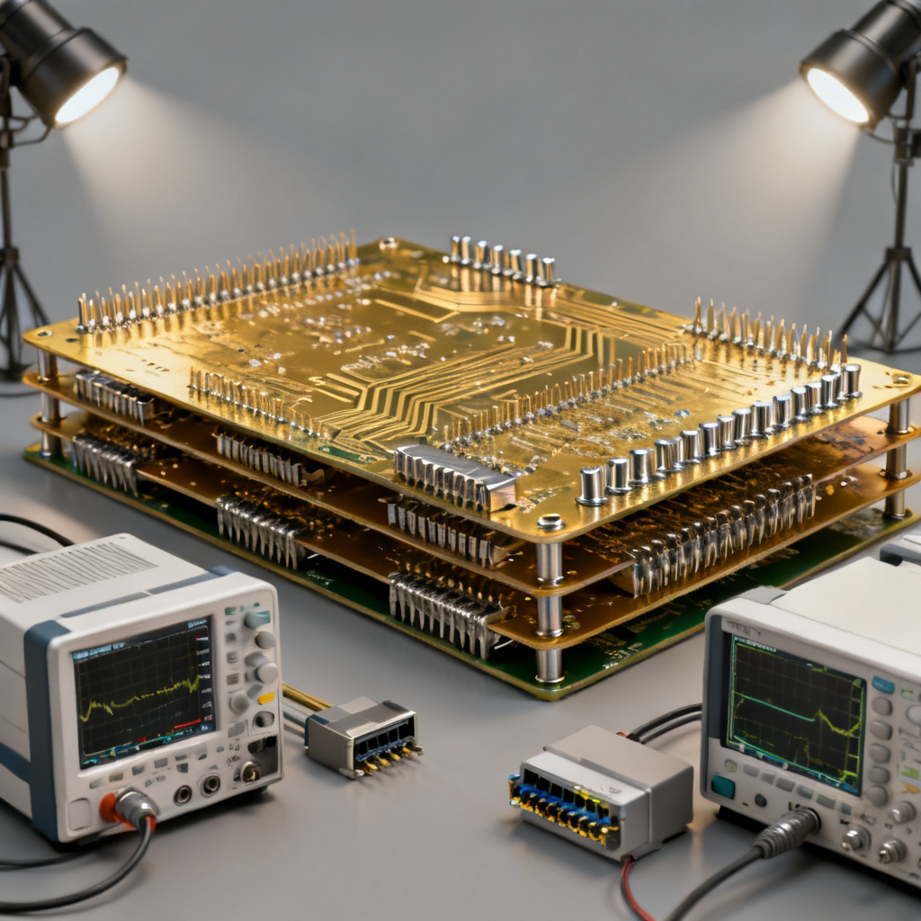
- Inspection: After insertion, perform a pull-test on sample pins (e.g., 10N minimum retention force). Use X-ray inspection to check for barrel cracks.
Back-Drilling Quality Control
- Depth Verification: Use a depth gauge or X-ray to measure the residual stub length. A common acceptance criterion is < 0.2mm (8 mils).
- Deburring: After back-drilling, use a deburring tool or plasma cleaning to remove copper whiskers and resin residue.
- Electrical Test: Perform a Time Domain Reflectometry (TDR) test on a test coupon to measure impedance discontinuities caused by the back-drilled via. A good back-drill should show a smooth impedance profile.
Common Pitfalls in High-Speed Backplane PCB Design
| Pitfall | Cause | Solution |
|---|---|---|
| Resonant Notch at 8 GHz | Via stub too long (e.g., 45 mils in FR4) | Back-drill to < 10 mils stub length. |
| Press-Fit Pin Loose | PTH hole too large or plating too thin | Tighten hole tolerance to ±0.05mm; increase plating to 30 microns. |
| Barrel Cracks After Insertion | High CTE laminate or excessive insertion force | Use low-CTE material (e.g., Megtron 6); calibrate press force. |
| High Insertion Loss (> -3 dB at 20 GHz) | Lossy material (FR4) or long trace length | Switch to low-Df laminate; use shorter routing. |
| Back-Drill Depth Error | Poor CNC calibration or board warp | Use a test coupon to verify depth; ensure board flatness. |
Conclusion – The Path to a Reliable High-Speed Backplane PCB
Designing a high-speed backplane PCB is a balancing act between mechanical robustness and electrical performance. Press-fit technology provides a reliable, solderless connection, but demands strict control over hole sizes, plating, and material CTE. Via stub removal via back-drilling is non-negotiable for data rates above 10 Gbps, eliminating resonant notches that can cripple signal integrity.
By combining:
- Low-loss, high-Tg laminates
- Precision back-drilling with tight depth control
- Optimized press-fit pin and anti-pad geometries
- Rigorous manufacturing inspection (X-ray, TDR)
…you can create a backplane that delivers flawless performance from 1 Gbps to 112 Gbps.
Need a partner for your next high-speed backplane PCB project? Contact our engineering team today for a free DFM review and stack-up consultation. We specialize in press-fit and back-drilling with tolerances down to ±0.05mm.
FAQ: High-Speed Backplane PCBs – Press-Fit & Via Stub Removal
What is a high-speed backplane PCB?
A high-speed backplane PCB is a large, multi-layer board that serves as a communication backbone for high-speed digital systems, typically handling data rates from 10 Gbps to 112 Gbps per lane.
Why is via stub removal important in high-speed backplane PCBs?
Via stub removal is critical because a via stub acts as a transmission line stub at high frequencies, causing resonant notches and signal degradation. Back-drilling is the standard method for removing these stubs in high-speed backplane PCBs.
What is the difference between press-fit and soldered connectors?
Press-fit connectors use a compliant pin that creates a gas-tight mechanical joint without solder, offering better reliability and easier field repairs in high-speed backplane PCBs. Soldered connectors require heat and are more difficult to rework.
What materials are best for high-speed backplane PCBs?
Low-loss, high-Tg laminates like Megtron 6, Isola I-Tera, or Rogers 4350B are recommended for high-speed backplane PCBs due to their stable dielectric constant and low dissipation factor.
How do I ensure reliable press-fit connections?
Ensure tight PTH hole tolerances (±0.05mm), minimum 25 microns copper plating, and use high-Tg, low-CTE laminates. Proper insertion force calibration is also essential for high-speed backplane PCBs.