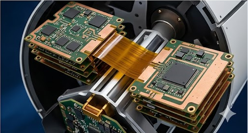
High-End PCB solutions are the backbone of modern AI, ADAS, radar, and LEO satellite systems. This comprehensive guide synthesizes the most authoritative industry insights to help you design and manufacture boards that meet the most demanding performance, reliability, and signal integrity requirements.
1. High-End PCB Design for AI & High-Performance Computing (HPC)
High-End PCB solutions for AI and HPC workloads—such as GPU clusters, TPUs, and inference accelerators—face extreme challenges in signal speed, power delivery, and density.
1.1 The Core Challenge: Signal Integrity & Power Integrity (SI/PI)
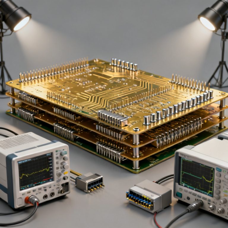
Expert sources confirm that AI PCBs typically require 20 to 30+ layers. The stackup must be carefully balanced. A common configuration uses multiple ground planes for isolation, dedicated power planes (often with split planes for multiple voltages like 0.8V, 1.2V, 1.8V), and multiple high-speed signal layers. Key insight: The stackup must be symmetrical to prevent warpage during lamination, a critical point for high-layer-count boards.
Standard FR-4 is insufficient. For AI, the industry standard is High-Tg (170°C-200°C) and Low Loss materials. MEGTRON 6 (from Panasonic), Isola I-Speed, and Rogers 4350B are frequently cited. These materials offer stable Dk (Dielectric Constant) and low Df (Dissipation Factor) at high frequencies (GHz range) and high temperatures.
For differential pairs (e.g., PCIe Gen 5/6, DDR5, 112Gbps SerDes), controlled impedance is non-negotiable. The target is typically 100Ω differential and 50Ω single-ended, with a tolerance of ±10% or tighter (±5% for critical nets). Microstrip and stripline topologies are used, with stripline preferred for reduced EMI.
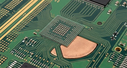
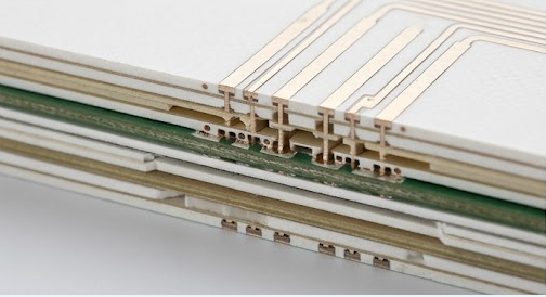
HDI (High-Density Interconnect) is mandatory. This includes:
- Microvias (laser-drilled): Typically 0.1mm to 0.15mm diameter, used for BGA fan-out and high-density routing.
- Buried & Blind Vias: Essential for complex layer transitions without using through-hole vias that block routing channels.
- Via Fill & Capping: Vias under BGA pads must be filled with conductive or non-conductive epoxy and capped with copper to prevent solder wicking and ensure flatness for solder joint reliability.
1.2 Thermal Management for AI & HPC
AI chips (e.g., NVIDIA A100/H100, AMD MI300) can consume 300W-700W+ per package. The PCB is a critical thermal path. High-End PCB solutions for thermal management include:
- Copper Coin / Inlay: Embedding a solid copper block directly into the PCB layer stack to conduct heat from the die to a heatsink.
- Thermal Vias: Arrays of small vias (e.g., 0.3mm pitch) placed directly under the chip’s thermal pad, filled with thermally conductive epoxy or plated with copper.
- Heavy Copper Layers: Using 2oz to 4oz (or more) copper on inner layers for power distribution and heat spreading.
- Metal Core PCBs (MCPCB): For extreme cases, an aluminum or copper base plate is used as the core, though this is less common for complex multi-layer AI boards.
2. High-End PCB Solutions for ADAS & Automotive Radar
ADAS and automotive radar (24 GHz, 77 GHz, 79 GHz) demand extreme reliability, safety (ISO 26262), and high-frequency performance. High-End PCB solutions in this domain must meet IPC Class 3 or Class 3/A standards.
2.1 The Unique Requirements of Automotive Electronics
The PCB must survive extreme temperature cycles (-40°C to +150°C), vibration, humidity, and salt spray. IPC Class 3 (High Reliability) or Class 3/A (Space/Aerospace) is the standard.
For 77GHz radar, the wavelength is ~3.9mm. PCB features must be smaller and more precise than ever. Standard FR-4 is completely unusable due to high loss and unstable Dk.
- Preferred Materials: Rogers RO3003, RO4835, and RO4000 series (e.g., RO4350B) are the gold standard. Taconic RF-35 and Isola Astra MT77 are also frequently recommended.
- Key Properties: Very low Df (e.g., 0.0013 for RO3003), stable Dk across frequency and temperature (e.g., Dk of 3.00 ± 0.04), and low moisture absorption.
The antenna layer is often a separate, low-loss laminate. The feed network (transmission lines) must be precisely routed with 50Ω impedance. Patch antennas and series-fed patch arrays are common. The ground plane directly below the antenna layer is critical for performance.
2.2 ADAS Processing & Power Electronics
ADAS processors (e.g., NVIDIA Drive Orin, Mobileye EyeQ) require high-speed DDR memory, PCIe, and Ethernet (100BASE-T1, 1000BASE-T1). This necessitates the same SI/PI techniques as AI, but with a stronger focus on EMI/EMC compliance (CISPR 25).
ADAS systems have multiple voltage rails (e.g., 12V, 5V, 3.3V, 1.8V, 0.8V). High-current power planes with thick copper (2oz-3oz) are needed. Buried capacitance (using thin laminates with high Dk) can help decouple power noise.
Manufacturing constraints include:
- Via-in-Pad (VIP): For dense BGA packages, VIP is required. Vias must be filled and planarized (copper-filled or resin-filled).
- Aspect Ratio: For thick boards (e.g., 1.6mm to 2.4mm) with small vias, the aspect ratio (board thickness / via diameter) must be controlled (typically ≤ 10:1 for reliable plating).
- Surface Finish: ENIG (Electroless Nickel Immersion Gold) is preferred for its flatness, solderability, and corrosion resistance. Immersion Silver and OSP are also used but offer less shelf life.
3. High-End PCB Solutions for Radar Systems (Beyond Automotive)
Military, aerospace, and industrial radar (including AESA and phased-array) have requirements even more stringent than automotive. High-End PCB solutions for these applications rely on ultra-low-loss PTFE-based laminates.
3.1 RF/Microwave PCB Design Principles
For X-band (8-12 GHz), Ku-band (12-18 GHz), and Ka-band (26.5-40 GHz), PTFE (Polytetrafluoroethylene) based laminates are the standard. Examples: Rogers RT/duroid 5880, 6002, 6010LM. These offer ultra-low loss and extremely stable Dk.
A common technique is to use a hybrid stackup – combining a low-loss RF laminate (e.g., Rogers 4350B) for the RF layer with a high-performance FR-4 (e.g., Isola 370HR) for the digital/power layers. This balances cost and performance. Critical: The materials must have compatible CTE (Coefficient of Thermal Expansion) to prevent delamination during reflow and thermal cycling.
For critical RF signals, a via structure that mimics a coaxial cable (signal via surrounded by ground vias) is used to ensure impedance control and isolation. Via fences (rows of closely spaced ground vias) and shield cans are used to isolate sensitive RF sections from digital noise. A solid, uninterrupted ground plane directly below the RF layer is non-negotiable.
3.2 Manufacturing Precision for Radar
For high-frequency circuits, line width and spacing tolerances must be ±0.0005 inches (12.5 microns) or better. Etching must be precise to maintain impedance. TDR (Time Domain Reflectometry) testing is mandatory to verify impedance of every critical trace.
ENIG is common. Immersion Gold (thicker than ENIG) or Gold Plating (for wire bonding) is used for high-reliability applications. HASL is avoided due to uneven surfaces.
Testing and inspection include:
- AOI (Automated Optical Inspection) for pattern defects.
- X-ray Inspection for inner layer alignment, via voids, and BGA solder joint quality.
- Flying Probe Testing for electrical continuity and isolation.
4. High-End PCB Solutions for LEO Satellites
LEO satellites (e.g., Starlink, OneWeb, CubeSats) operate in a harsh space environment: vacuum, extreme temperature swings, radiation, and vibration during launch. High-End PCB solutions for space must meet IPC Class 3/A and NASA/ECSS standards.
4.1 Space-Grade Materials & Design
Materials must have low outgassing (Total Mass Loss < 1.0%, Collected Volatile Condensable Material < 0.1%) per ASTM E595. Standard FR-4 is unacceptable.
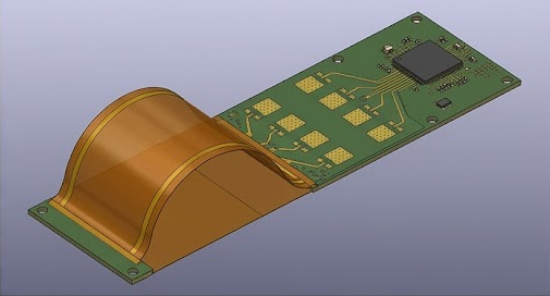
- Polyimide (e.g., DuPont Pyralux, Rogers 3000 series) for flexible and rigid-flex PCBs. Polyimide has excellent thermal stability and low outgassing.
- High-Tg FR-4 variants (e.g., Isola 370HR, Nelco 4000-13) are used for rigid boards, but must be qualified for outgassing.
- Ceramic-filled PTFE (e.g., Rogers RO3003, RT/duroid 6002) for RF and antenna sections.
There is no convection cooling in vacuum. Heavy copper (up to 4oz or more) and thermal vias are essential. The PCB itself can be coated with high-emissivity coatings (e.g., black polyimide) to radiate heat to space. The PCB’s CTE must be matched to the component’s CTE (especially for large BGAs) to prevent solder joint cracking during thermal cycling (-55°C to +125°C). Copper-invar-copper (CIC) cores are sometimes used to match CTE.
4.2 Radiation Hardening & Reliability
The PCB design can mitigate radiation effects. Techniques include:
- Guard rings around sensitive circuits.
- Decoupling capacitors close to every power pin.
- Redundant routing for critical signals.
The PCB must be mechanically robust. Stiffeners (e.g., aluminum or FR-4) are added to thin flex sections. Conformal coating (e.g., Parylene C, silicone) protects against moisture, dust, and tin whiskers.
Manufacturing standards include IPC Class 3/A, NASA-STD-8739, or ECSS-Q-ST-70-11. This includes:
- 100% inspection of all solder joints.
- X-ray inspection for voids and solder joint quality.
- Thermal cycling testing (e.g., 100 cycles from -55°C to +125°C).
- Burn-in testing (e.g., 168 hours at 85°C).
4.3 PCB Design for LEO Communication Systems
LEO satellites use phased-array antennas (e.g., for Ka-band user links). These require very large, multi-layer PCBs (e.g., 40” x 40”) with thousands of microvias and tight tolerances. Heavy copper (2oz-6oz) is used for power planes to minimize I²R losses. Embedded passive components (resistors, capacitors) are sometimes used to save space and weight.
Many LEO satellites use rigid-flex designs to save weight and reduce connector count. The flex layers are typically polyimide. The bend radius must be carefully controlled (e.g., >10x the flex thickness).
Comparison: High-End PCB Solutions vs. Standard FR-4
| Parameter | High-End PCB Solutions | Standard FR-4 |
|---|---|---|
| Material Type | Rogers, Isola, Taconic, Polyimide, PTFE | Standard epoxy-glass (FR-4) |
| Layer Count | 20 to 40+ layers | 2 to 8 layers typical |
| Max Frequency | Up to 100+ GHz (mmWave) | Below 1 GHz (unstable above) |
| Thermal Management | Heavy copper, thermal vias, copper coin/inlay | Limited to standard copper thickness |
| Reliability Standard | IPC Class 3, Class 3/A, NASA, ECSS | IPC Class 2 typical |
| Impedance Tolerance | ±5% or better | ±10% typical |
FAQ: High-End PCB Solutions for AI, ADAS, Radar & LEO Satellite
What materials are best for High-End PCB solutions in AI applications?
For AI and HPC, High-End PCB solutions use low-loss, high-Tg materials like MEGTRON 6, Isola I-Speed, and Rogers 4350B to ensure signal integrity and thermal reliability.
How do High-End PCB solutions differ for ADAS radar vs. LEO satellite?
ADAS radar High-End PCB solutions focus on automotive-grade reliability (IPC Class 3) and mmWave performance (77 GHz), while LEO satellite solutions prioritize space-grade outgassing, radiation hardening, and extreme thermal cycling tolerance.
What is the typical layer count for High-End PCB solutions in LEO satellites?
LEO satellite High-End PCB solutions often use 20 to 40+ layers, with heavy copper (2oz-6oz) for power distribution and rigid-flex designs for weight savings.
Why is controlled impedance critical in High-End PCB solutions for radar?
Controlled impedance (±5% tolerance) is essential in radar High-End PCB solutions to maintain signal integrity at GHz frequencies, preventing reflections and power loss in antenna feed networks.
What testing is required for High-End PCB solutions in space applications?
Space-grade High-End PCB solutions require 100% inspection, X-ray for voids, thermal cycling (-55°C to +125°C), and burn-in testing per NASA-STD-8739 or ECSS standards.
Glossary of Key Terms
- Dk (Dielectric Constant): A material property that affects signal propagation speed; stable Dk is critical for High-End PCB solutions in high-frequency designs.
- Df (Dissipation Factor): A measure of signal loss in a dielectric; low Df is essential for High-End PCB solutions in radar and satellite communications.
- CTE (Coefficient of Thermal Expansion): The rate at which a material expands with temperature; matching CTE prevents delamination