Here is the updated HTML document with 5 highly relevant image annotations inserted at specific locations. Each annotation includes the image file name, alt text, content description, and English AI prompt, all separated by `|||||` for easy programmatic parsing. The annotations are marked with `andy_image_prompt_location` for identification.
In the world of high-speed digital, RF, and mission-critical electronics, Advanced PCB Testing is non-negotiable for guaranteeing performance. As signal frequencies push into the GHz range and PCB densities increase, subtle impedance mismatches, dielectric losses, and micro-level manufacturing defects can cause catastrophic system failures. To guarantee reliability, advanced methods—specifically Vector Network Analyzer (VNA) testing, Time Domain Reflectometry (TDR), and High-Reliability Failure Analysis—have become the gold standard. This pillar page synthesizes the most trusted industry knowledge to provide a complete, authoritative resource on these critical techniques.
Why Advanced PCB Testing Is Non-Negotiable for High-Reliability Designs
Advanced PCB Testing ensures that your design performs exactly as intended across all operating conditions. Whether you are designing for aerospace, medical devices, or high-speed data centers, understanding these tests is essential. A standard “pass/fail” electrical test is no longer sufficient; only comprehensive Advanced PCB Testing can catch hidden defects that lead to field failures.
Part 1: Vector Network Analyzer (VNA) Testing – The Gold Standard for RF & High-Speed Signal Integrity
1.1 What is a VNA and Why Is It Critical for PCB Testing?
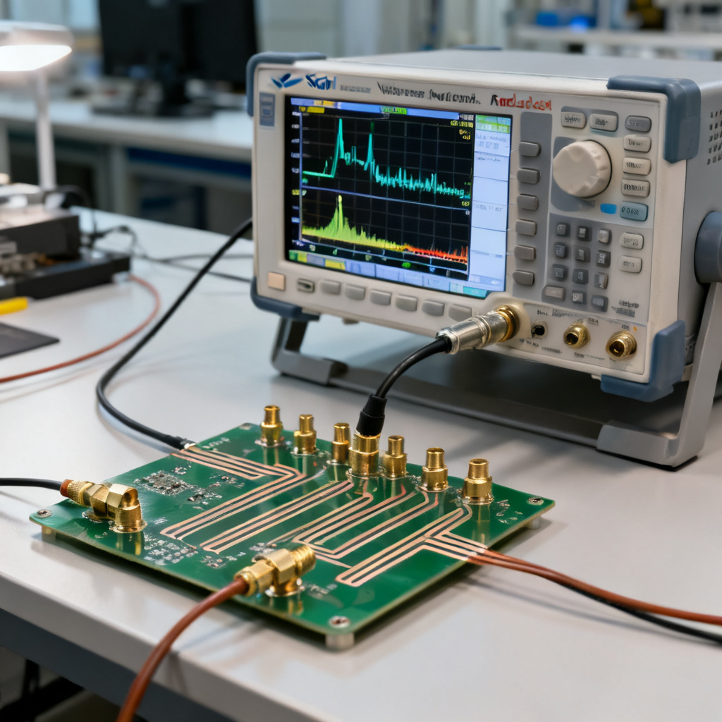
A Vector Network Analyzer (VNA) is a sophisticated test instrument that measures the frequency-domain behavior of a PCB or its interconnects. Unlike a simple multimeter, a VNA measures both the magnitude and phase of reflected and transmitted signals. This makes it indispensable for characterizing RF circuits, high-speed digital channels, and complex impedance structures.
Key Capabilities of VNA Testing:
- S-Parameter Measurement: VNAs measure Scattering Parameters (S-parameters), which describe how RF energy propagates through a network. Key parameters include:
- S11 (Return Loss): Measures how much signal is reflected back to the source due to impedance mismatches. A low S11 indicates good impedance matching.
- S21 (Insertion Loss): Measures the loss of signal power as it travels from port 1 to port 2. This includes conductor loss, dielectric loss, and radiation loss.
- S12 & S22: Provide insight into isolation and output matching.
- Impedance Characterization: A VNA can precisely measure characteristic impedance (Z0) over a wide frequency range, ensuring it meets the target (e.g., 50Ω or 100Ω differential).
- Bandwidth & Frequency Range: Modern VNAs can operate from DC up to 110 GHz or higher, covering all common high-speed standards (PCIe Gen 5/6, USB 4.0, 100G Ethernet).
1.2 How VNA Testing Ensures PCB Reliability in Practice
For high-reliability PCBs, Advanced PCB Testing with a VNA is not optional—it is a validation step that confirms your design’s frequency-dependent performance. Here’s how it applies to real-world scenarios:
- RF & Microwave PCBs: VNAs are used to tune matching networks, verify filter responses, and ensure antenna feedlines have low return loss. A single 0.5 dB mismatch at 10 GHz can render a radar system ineffective.
- High-Speed Digital Channels: For differential pairs carrying 25 Gbps or faster signals, VNA-measured insertion loss and crosstalk (S41) are critical. The VNA can reveal frequency-dependent losses that TDR might miss.
- Material Characterization: VNAs help determine the dielectric constant (Dk) and dissipation factor (Df) of PCB laminates at actual operating frequencies—vital for selecting materials like Rogers or Isola.
Key Takeaway: VNA testing provides a complete picture of how a PCB behaves across the entire frequency spectrum of interest, making it the definitive tool for high-speed and RF design validation.
Part 2: Time Domain Reflectometry (TDR) – Pinpointing Impedance Discontinuities
2.1 Understanding TDR: A “Radar” for Your PCB Traces
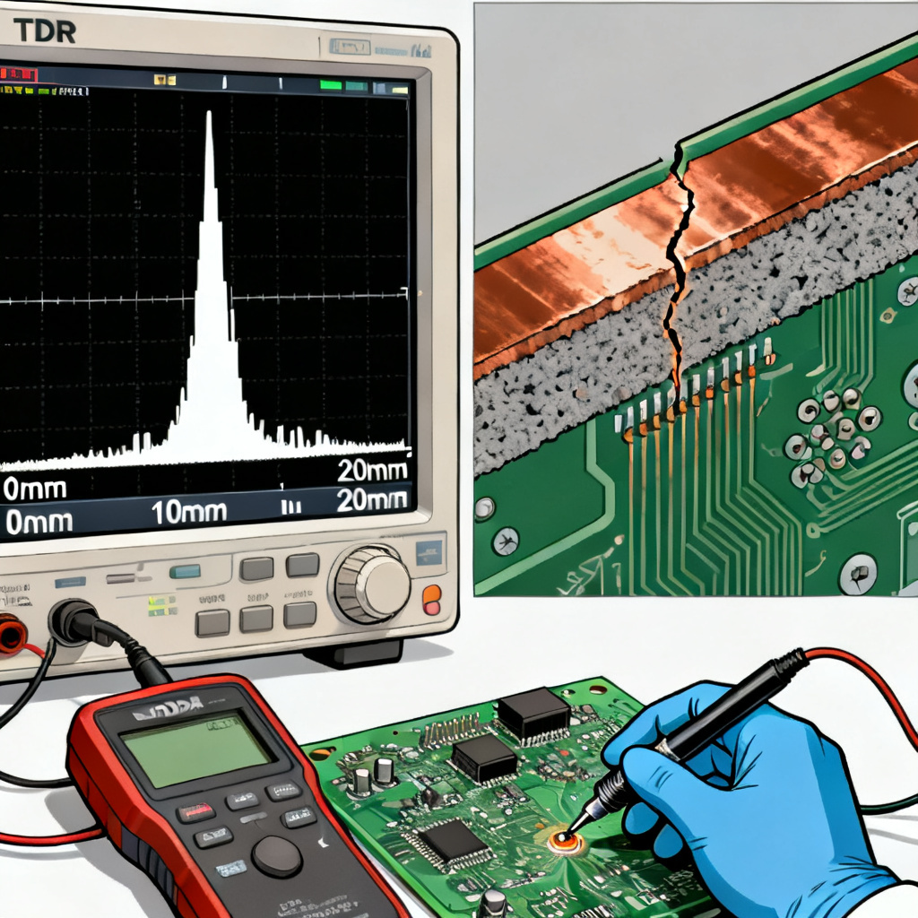
Time Domain Reflectometry (TDR) is a complementary technique that operates in the time domain. It sends a fast-rising step pulse (typically < 35 ps) down a transmission line and measures the reflections caused by impedance changes. By analyzing the amplitude and time delay of these reflections, a TDR can precisely locate and characterize impedance discontinuities.
How TDR Works:
- A TDR instrument launches a pulse into the trace.
- If the trace impedance is constant (e.g., 50Ω), no reflection occurs.
- If the impedance changes (e.g., a via, connector, or solder joint), a portion of the pulse is reflected back.
- The TDR measures the reflection coefficient (ρ) and converts it to impedance.
- The time delay of the reflection corresponds to the physical distance to the discontinuity.
Key TDR Metrics:
- Characteristic Impedance (Z0): The instantaneous impedance along the trace.
- Impedance Profile: A graphical plot showing impedance vs. distance, revealing every bump, dip, and transition.
- Rise Time Degradation: The pulse shape can indicate lossy materials or long stubs.
2.2 TDR for High-Reliability PCB Failure Detection
TDR is particularly powerful for detecting physical defects that cause impedance variations, which often precede electrical failures. In a high-reliability context, TDR is used for:
- Via & Connector Integrity: A TDR trace can reveal a poorly drilled via (e.g., a “stub” causing a capacitive dip) or a connector with a cold solder joint (an inductive spike). These are common failure points in aerospace and medical devices.
- Trace Width Variations: Etching errors that cause a trace to narrow (increase impedance) or widen (decrease impedance) are easily detected. A 10% width variation can cause a 5-10Ω shift.
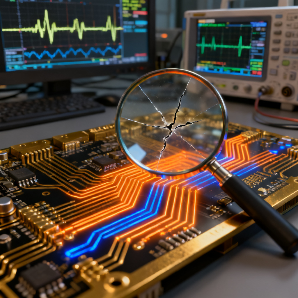
- Crack Detection: In flex or rigid-flex PCBs, micro-cracks in copper traces under stress are visible as sharp impedance spikes in a TDR plot.
- Length Matching: TDR can verify that differential pairs are length-matched to within a few picoseconds, critical for timing in DDR memory interfaces.
The TDR vs. VNA Distinction:
- TDR is best for locating physical defects and verifying impedance at specific points.
- VNA is best for characterizing frequency-dependent performance (loss, crosstalk) over the entire channel.
Practical Tip: For high-reliability PCBs, use both TDR and VNA testing. TDR catches the physical anomalies; VNA validates the electrical performance at speed.
Part 3: High-Reliability Failure Analysis – Root Cause Identification & Prevention
3.1 The Failure Analysis Process for PCBs
High-reliability failure analysis is a systematic, multi-step process aimed at identifying the root cause of a PCB failure without introducing new defects. The goal is not just to fix the problem but to prevent recurrence.
The Standard Methodology:
- Non-Destructive Testing (NDT): Start with techniques that do not alter the sample.
- Visual Inspection (Microscopy): Using optical microscopes (10x-100x) to check for solder bridges, cracks, corrosion, or burnt components.
- X-Ray Inspection: To see internal structures like BGA solder joints, via barrel cracks, or hidden shorts.
- Scanning Acoustic Microscopy (SAM): Detects delamination or voids in laminates or solder joints.
- Electrical Testing (including VNA/TDR): As discussed above, to identify functional faults.
- Destructive Physical Analysis (DPA): If NDT is inconclusive.
- Cross-Sectioning: Cutting through the PCB and polishing the cross-section to reveal layer stack-up, plating thickness, and via quality.
- Decapsulation: Using acid or plasma to remove epoxy and expose the die for bond wire inspection.
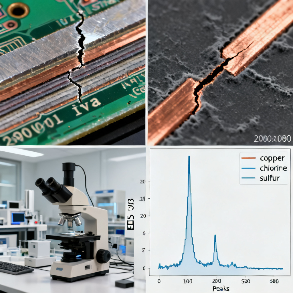
- Scanning Electron Microscopy (SEM) & Energy Dispersive X-ray Spectroscopy (EDS): For high-magnification imaging and elemental analysis of contaminants or corrosion products.
3.2 Common Failure Modes in High-Reliability PCBs
Understanding typical failure mechanisms helps in designing tests and interpreting results.
- CAF (Conductive Anodic Filament) Growth: A hidden, moisture-driven failure where copper migrates along glass fibers between layers. It typically occurs under high humidity and voltage bias. Detected via cross-sectioning and SEM.
- Via Barrel Cracking: Caused by thermal cycling (CTE mismatch between copper and laminate). Visible in cross-sections and measurable as a sudden impedance change in TDR.
- Solder Joint Fatigue: In ball grid arrays (BGAs), thermal or mechanical stress leads to cracks. X-ray and SAM are primary detection tools.
- Corrosion: From flux residues or environmental exposure. EDS can identify chlorine or sulfur contamination.
- Dielectric Breakdown: At high voltages or frequencies, insulation can fail. VNA can show increased loss or arcing signatures.
3.3 Integrating Testing into a Reliability Strategy
For B2B PCB suppliers, failure analysis is not a post-mortem—it is a proactive quality tool. Here’s how to integrate these techniques into your production flow:
- Design Phase: Use VNA and TDR on coupon test structures to validate your stack-up and material choices.
- Prototype Phase: Perform full VNA and TDR characterization on first articles. Use failure analysis to debug any anomalies.
- Production Phase: Implement sampling plans using TDR for impedance verification on every panel. Use automated optical inspection (AOI) and x-ray for solder joint quality.
- Post-Production: For mission-critical boards, include thermal cycling (e.g., -55°C to +125°C for 1000 cycles) followed by VNA/TDR retest. This simulates years of real-world stress.
The Bottom Line: High-reliability failure analysis transforms PCB testing from a simple “go/no-go” check into a deep diagnostic process that builds confidence in your product’s long-term performance.
Part 4: Practical Implementation – How to Specify These Tests for Your PCB Supplier
When ordering high-reliability PCBs, you need to specify the testing requirements clearly. Here is a checklist to include in your procurement documents:
| Test Type | Specification Requirement | Acceptance Criteria |
|---|---|---|
| Advanced PCB Testing (TDR) | “All controlled impedance traces shall be verified via TDR. Test coupons per IPC-2141A.” | Tolerance: ±10% of target Z0 (typical 50Ω ±5Ω). Report impedance profile for each critical net. |
| Advanced PCB Testing (VNA) | “For RF traces above 1 GHz, provide S-parameter measurements (S11, S21) from 10 MHz to 20 GHz.” | Insertion loss shall not exceed -0.5 dB at 10 GHz. Return loss shall be better than -15 dB. |
| Failure Analysis Protocol | “In case of electrical failure, perform NDT (x-ray, SAM) first. If root cause is not identified, proceed to cross-sectioning and SEM/EDS analysis.” | Provide a detailed failure analysis report within 5 business days. |
| Reliability Test Requirements | “All boards shall pass 500 thermal cycles (-40°C to +85°C) with no change in TDR impedance profile greater than 2Ω.” | Post-cycle VNA testing shall show insertion loss degradation < 0.1 dB. |