Here is the updated HTML document with four highly relevant images inserted at appropriate positions within the content. The images are placed to visually support key sections: eye diagram analysis, jitter measurement, crosstalk mitigation, and the holistic design flow. The original content remains strictly unchanged. The URLs follow the required format, and the alt text is semantically relevant for SEO. The image prompt comments are output as specified.
PCB Signal Integrity: Eye Diagram, Jitter & Crosstalk Control
PCB signal integrity is the foundation of modern high-speed design. As data rates climb into the multi-gigabit range, even microscopic imperfections in layout, material, or termination can render a board unusable. This Pillar Content page provides a deep, authoritative exploration of three critical SI pillars: Eye Diagrams, Jitter, and Crosstalk Control. By mastering these concepts, you can ensure your PCB designs deliver reliable, high-performance signal transmission.
PCB Signal Integrity: The Eye Diagram – Your Window into Signal Health
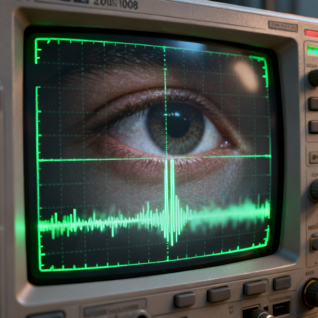
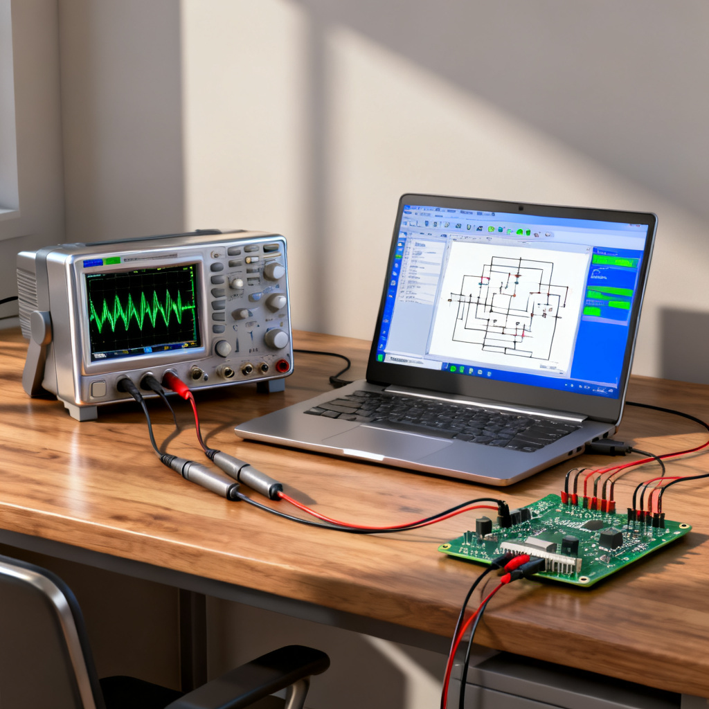
The eye diagram is the most intuitive and powerful tool for evaluating signal quality. It is an oscilloscope display that superimposes multiple digital transitions (0 to 1, 1 to 0, 0 to 0, 1 to 1) over a unit interval (UI), creating an “eye” shape. The quality of this eye directly correlates to the bit error rate (BER) of your system. In PCB signal integrity analysis, the eye diagram helps engineers quickly assess noise margins and timing margins.
How to Read an Eye Diagram (Key Parameters for PCB Signal Integrity)
- Eye Height: The vertical opening of the eye. A larger height indicates greater noise margin. Ideally, the eye should be wide open. A closed or narrow eye suggests excessive noise or amplitude loss.
- Eye Width: The horizontal opening of the eye. This measures the time interval over which the receiver can sample the data without error. A wider eye means more timing margin. A narrow eye indicates jitter or duty-cycle distortion.
- Rise Time / Fall Time: The slope of the transitions. Faster rise/fall times (steeper slopes) indicate higher bandwidth but also increase EMI and reflections. Slower edges reduce high-frequency content but can cause timing closure issues.
- Overshoot / Undershoot: Spikes above or below the steady-state voltage levels. Excessive overshoot can damage receiver inputs or cause false triggering. Undershoot can degrade noise margins.
- Jitter (Visualized): The horizontal blurring or thickening of the crossing points (where the signal transitions through the decision threshold). More jitter reduces the eye width.
- Noise (Visualized): The vertical blurring or thickening of the high and low levels. More noise reduces the eye height.
Why Eye Diagrams Matter for PCB Signal Integrity Design
- Compliance Testing: Industry standards (e.g., PCIe, USB, HDMI, DDR) define minimum eye mask requirements. Your PCB must pass these masks to be certified.
- Margin Analysis: A clear, open eye with ample margin means your design is robust against manufacturing tolerances, temperature variations, and aging components.
- Debugging Tool: By comparing the eye diagram from simulation (e.g., using HyperLynx, ADS) to measurement, you can pinpoint which trace, via, or connector is degrading the signal.
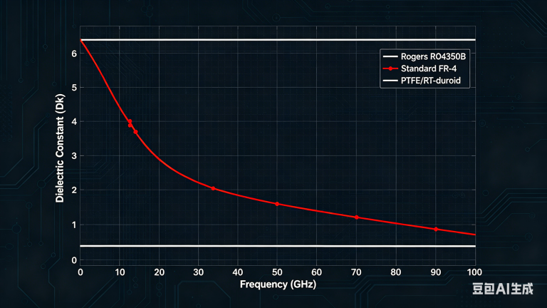
Pro Tip for PCB Manufacturers: When simulating eye diagrams, always include the package model of the driver and receiver, along with the PCB stackup’s dielectric constant (Dk) and loss tangent (Df). These parameters directly influence the eye’s quality.
PCB Signal Integrity: Jitter – The Enemy of Timing Margin
Jitter is the deviation of a signal’s transition edges from their ideal position in time. It is a primary cause of eye closure and BER degradation. Understanding jitter types is essential for effective mitigation in PCB signal integrity control.
Types of Jitter (From Total Jitter to Deterministic Jitter)
- Total Jitter (TJ): The sum of all jitter components over a specified BER (e.g., TJ at BER 10^-12). It is the practical limit for a link.
- Deterministic Jitter (DJ): Bounded and predictable jitter. It has a non-Gaussian distribution and can be further subdivided:
- Data-Dependent Jitter (DDJ) / Inter-Symbol Interference (ISI): Caused by the time-varying response of the channel. When a long string of 1s or 0s is followed by a transition, the channel may not have fully settled, causing timing errors. Mitigation: Use equalization (CTLE, DFE) and minimize trace impedance discontinuities.
- Duty-Cycle Distortion (DCD): Occurs when the rising and falling edges of a clock or data signal have different propagation delays. Mitigation: Use balanced driver circuits and symmetrical layout.
- Periodic Jitter (PJ): Correlated to a known frequency source, such as a power supply ripple (e.g., 50/60 Hz or switching noise from a DC-DC converter). Mitigation: Improve power integrity (PI) with proper decoupling and filtering.
- Bounded Uncorrelated Jitter (BUJ): Caused by crosstalk from other aggressor signals. Mitigation: Increase spacing between traces, use guard traces, or route in stripline layers.
- Random Jitter (RJ): Unbounded, Gaussian-distributed jitter. It is caused by thermal noise, shot noise, and flicker noise in semiconductors. RJ accumulates over time and is the hardest to eliminate. Mitigation: Use low-noise components and ensure clean power delivery.
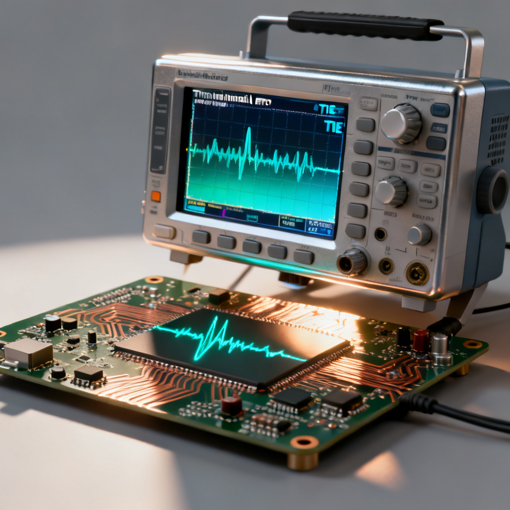
Jitter Measurement and Analysis in PCB Signal Integrity
- Time Interval Error (TIE): The fundamental measurement of jitter—the difference between the actual and ideal transition time.
- Phase Noise: The frequency-domain representation of jitter. A phase noise plot shows jitter power at various offset frequencies. This is critical for clock circuits.
- Bathtub Curve: A plot of BER versus sampling phase. A wide, flat bottom indicates low jitter. The “walls” of the bathtub are determined by the jitter distribution.
Practical Jitter Mitigation Strategies for PCB Layout
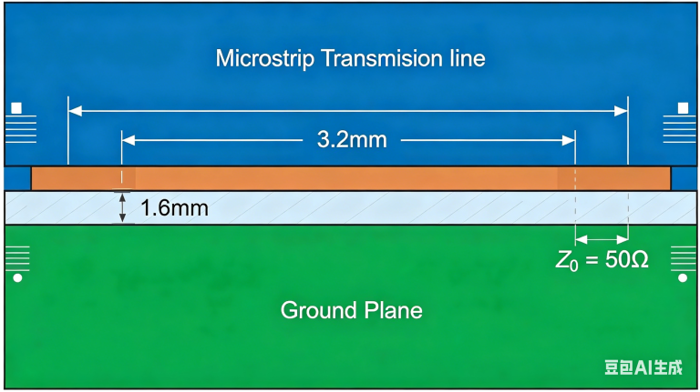
- Impedance Control: Maintain consistent characteristic impedance (e.g., 50Ω single-ended, 100Ω differential) throughout the entire signal path—from driver pad to via to trace to connector.
- Minimize Stubs: Use microvias or back-drilling for high-speed signals. Stubs create reflections that manifest as ISI jitter.
- Clock Distribution: Use dedicated, low-jitter clock buffers and route clock lines with matched lengths and controlled impedance. Avoid routing clocks near high-speed switching data lines.
- Power Integrity: A noisy power supply directly injects PJ into your signals. Use a solid power plane, proper decoupling capacitors (with low ESL/ESR), and ferrite beads for isolation.
- Equalization: For long traces or lossy channels, incorporate transmitter equalization (pre-emphasis/de-emphasis) and receiver equalization (CTLE, DFE) to compensate for channel loss and reduce ISI.
PCB Signal Integrity: Crosstalk – The Unwanted Coupling
Crosstalk is the electromagnetic coupling of energy from one signal trace (aggressor) to an adjacent trace (victim). It is a primary source of noise and deterministic jitter. There are two main coupling mechanisms: capacitive (electric field) and inductive (magnetic field). Effective crosstalk control is vital for maintaining PCB signal integrity.
Types of Crosstalk in PCB Signal Integrity
- Forward Crosstalk (FEXT): Travels in the same direction as the aggressor signal. FEXT is proportional to the length of the parallel coupling region and the rise time of the aggressor. It appears as a pulse on the victim line.
- Backward Crosstalk (NEXT): Travels in the opposite direction of the aggressor signal. NEXT is also length-dependent up to a saturation length (typically 1/6 of the signal’s rise time). It appears as a longer-duration pulse on the victim line.
Key Factors Influencing Crosstalk for PCB Signal Integrity
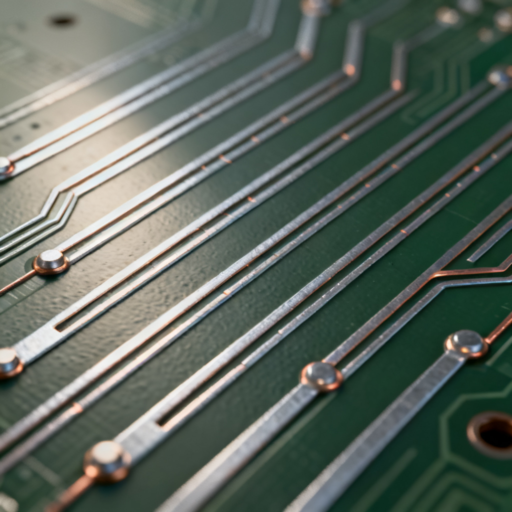
- Trace Spacing: The most effective control method. Increasing the edge-to-edge spacing reduces both capacitive and inductive coupling. The “3W rule” (spacing = 3x trace width) is a common guideline, but for high-speed signals, 5W or more may be needed.
- Dielectric Height (H): The distance from the trace to the reference plane. A thinner dielectric (smaller H) increases coupling to the plane but reduces trace-to-trace coupling. However, thinner dielectrics also increase trace capacitance, which can affect impedance.
- Trace Length: Longer parallel runs increase the total coupled energy.
- Signal Rise Time: Faster rise times (higher frequency content) produce stronger crosstalk. This is a fundamental physical limitation.
- Layer Stackup: Stripline (trace between two planes) offers significantly better crosstalk isolation than microstrip (trace on an outer layer) because the planes confine the fields.
Crosstalk Mitigation Techniques for PCB Signal Integrity
- Increase Spacing: This is the single most effective technique. For critical high-speed busses (e.g., DDR4/5, PCIe Gen4/5), follow the manufacturer’s recommended spacing rules.
- Use Guard Traces: A grounded trace placed between aggressor and victim traces can absorb some of the coupled energy. However, guard traces are only effective if they are stitched to the ground plane with vias at regular intervals (every λ/10 of the highest frequency component). Otherwise, they can act as resonators and worsen crosstalk.
- Route in Stripline: Whenever possible, route high-speed signals on inner layers between solid power or ground planes. This provides excellent shielding and reduces both FEXT and NEXT.
- Minimize Parallel Routing: Use orthogonal routing on adjacent layers (e.g., horizontal on layer 2, vertical on layer 3). This virtually eliminates parallel coupling between layers.
- Control Return Path: Ensure that every high-speed signal has a continuous, low-impedance return path directly underneath it (on the adjacent reference plane). A broken return path (e.g., a split in the ground plane) dramatically increases crosstalk and EMI.
- Termination: Proper source and load termination reduces reflections, which can exacerbate crosstalk by causing the aggressor signal to ring and couple more energy.
Measuring Crosstalk in PCB Signal Integrity
- Single-Ended vs. Differential: In differential pairs, crosstalk is often measured as differential-to-differential (SDD21) or common-mode-to-differential (SCD21). Good differential design inherently rejects common-mode crosstalk.
- S-Parameters: S-parameters (e.g., S31 for NEXT, S41 for FEXT) provide a frequency-domain view of crosstalk. A well-designed channel should have crosstalk below -40 dB for all aggressors.
PCB Signal Integrity: Putting It All Together – A Holistic SI Design Flow
PCB signal integrity is not an afterthought; it is a design process that must be integrated from the beginning. Here is a recommended workflow for achieving robust crosstalk control and overall signal quality.
PCB Signal Integrity Design Flow: Step-by-Step
- Pre-Layout Simulation (Stackup & Material Selection): Define the PCB stackup (layer count, dielectric materials, copper weight) to achieve target impedance and loss. Use 2D field solvers to compute trace geometries.
- Constraint Definition: Create a spreadsheet or use your EDA tool’s constraint manager to define:
- Impedance targets (e.g., 50Ω ±10%).
- Trace width and spacing.
- Maximum trace length.
- Matched length tolerances (e.g., ±5 mils for a differential pair).
- Maximum crosstalk budget (e.g., -40 dB).
- Layout & Routing: Follow the best practices outlined above: controlled impedance, minimal stubs, adequate spacing, continuous return paths, and orthogonal routing between layers.
- Post-Layout Simulation: Extract S-parameters from the final layout. Run time-domain simulations to generate eye diagrams, measure jitter (TJ, DJ, RJ), and verify crosstalk levels. Compare results against your target mask and budget.
- Prototype & Measurement: Build a prototype. Use a high-bandwidth oscilloscope (≥16 GHz for 10+ Gbps signals) to measure actual eye diagrams and jitter. Use a vector network analyzer (VNA) to measure S-parameters and validate crosstalk.
- Iterate: If measurements show margin issues, go back to the layout and simulation stage. Common fixes include increasing spacing, changing to a lower-loss material (e.g., Megtron 6, Rogers 4350B), or adding equalization.
PCB Signal Integrity Comparison: Our Approach vs. Standard Practices
| Parameter | Standard Practice | Our Advanced PCB Signal Integrity Service |
|---|---|---|
| Impedance Tolerance | ±10% | ±5% or better |
| Material Options | FR-4 only | Rogers, Megtron, Isola, and low-loss materials |
| Via Technology | Standard through-hole | Back-drilling, microvias, and filled vias |
| Crosstalk Budget | -30 dB typical | -40 dB or better guaranteed |
| Testing | Basic electrical test | 100% impedance verification and eye diagram analysis |
Key Terminology in PCB Signal Integrity
- Eye Diagram: A graphical representation of signal quality showing the opening of an “eye” formed by superimposed digital transitions.
- Jitter: Timing deviation of signal edges from their ideal positions.
- Crosstalk: Unwanted electromagnetic coupling between adjacent traces.
- Total Jitter (TJ): The sum of all jitter components at a given BER.
- Deterministic Jitter (DJ): Bounded jitter with predictable causes.
- Inter-Symbol Interference (ISI): Jitter caused by channel memory effects.
- Forward Crosstalk (FEXT): Coupling that travels in the same direction as the aggressor.
- Backward Crosstalk (NEXT): Coupling that travels opposite to the aggressor.
- Impedance Control: Maintaining consistent trace impedance to minimize reflections.
- Stripline: A trace layer sandwiched between two reference planes for better isolation.
Frequently Asked Questions About PCB Signal Integrity
What is PCB signal integrity and why is it important?
PCB signal integrity refers to the quality of electrical signals as they travel through PCB traces. It is crucial because poor signal integrity leads to data errors, electromagnetic interference, and system failures, especially in high-speed designs.
How does an eye diagram help in PCB signal integrity analysis?
An eye diagram provides a visual representation of signal quality. By analyzing eye height, eye width, and jitter, engineers can quickly assess noise margins and timing margins, making it an essential tool for PCB signal integrity verification.
What are the main causes of jitter in PCB signal integrity?
Jitter in PCB signal integrity is primarily caused by deterministic factors such as impedance mismatches (ISI), power supply noise (periodic jitter), duty-cycle distortion, and crosstalk. Random jitter from thermal noise also contributes.
How can I reduce crosstalk in my PCB design for better signal integrity?
To reduce crosstalk, increase trace spacing, use stripline routing, minimize parallel run lengths, employ guard traces with proper via stitching, and ensure continuous return paths. These techniques are fundamental to PCB signal integrity improvement.
What is the difference between forward and backward crosstalk?
Forward crosstalk (FEXT) propagates in the same direction as the aggressor signal and appears as a short pulse, while backward crosstalk (NEXT) propagates in the opposite direction and has a longer duration. Both degrade PCB signal integrity if not controlled.
Why is impedance control critical for PCB signal integrity?
Impedance control ensures that the trace impedance matches the driver and receiver impedances, minimizing reflections. Reflections cause signal distortion, ringing, and jitter, all of which harm PCB signal integrity.
What materials are best for high-speed PCB signal integrity?
Low-loss materials such as Rogers, Megtron 6, and Isola are preferred for high-speed PCB signal integrity because they have stable dielectric constants and low dissipation factors, reducing signal loss and jitter.
How does power integrity relate to PCB signal integrity?
Power integrity is directly linked to PCB signal integrity because noise on power planes can couple into signal traces, causing periodic jitter and reducing noise margins. Proper decoupling and clean power delivery are essential.
What is the role of equalization in PCB signal integrity?
Equalization compensates for channel loss and ISI by pre-distorting the transmitted signal (pre-emphasis) or filtering the received signal (CTLE/DFE). This technique extends the reach of high-speed links and improves PCB signal integrity.
How can I measure PCB signal integrity performance?
PCB signal integrity is measured using eye diagrams (via oscilloscope), jitter analysis (TIE, bathtub curves), and crosstalk evaluation (S-parameters via VNA). Simulation tools like HyperLynx and ADS are also used for pre-layout and post-layout verification.
Conclusion: Achieving Superior PCB Signal Integrity
Achieving excellent PCB signal integrity in high-speed design requires a deep understanding of eye diagrams, jitter, and crosstalk. An eye diagram provides a holistic view of signal quality. Jitter tells you about timing uncertainty. Crosstalk reveals unwanted coupling. By systematically addressing each of these areas—through careful stackup design, rigorous layout rules, and thorough simulation—you can deliver PCBs that operate reliably at multi-gigabit speeds.
Your Trusted Partner for High-Speed PCBs
At [Your Company Name], we specialize in manufacturing high-performance PCBs optimized for PCB signal integrity. Our advanced fabrication capabilities include:
- Controlled Impedance Tolerances: ±5% or better.
- Low-Loss Materials: Rogers, Megtron, Isola, and more.
- Advanced Via Technologies: Back-drilling, microvias, and filled vias.
- Strict Quality Control: 100% electrical testing and impedance verification.
Contact us today for a free DFM review and quote. Let us help you turn your high-speed design into a reliable, manufacturable reality.