High-Speed PCB Design: SI/PI Simulation & Via Modeling Guide is the definitive resource for engineers seeking first-pass success in multi-GHz designs. As data rates exceed 1 Gbps, traditional layout rules fail; mastering signal integrity, power integrity, and via modeling is no longer optional but essential for reliable high-speed PCB design.
Signal Integrity Foundation for High-Speed PCB Design
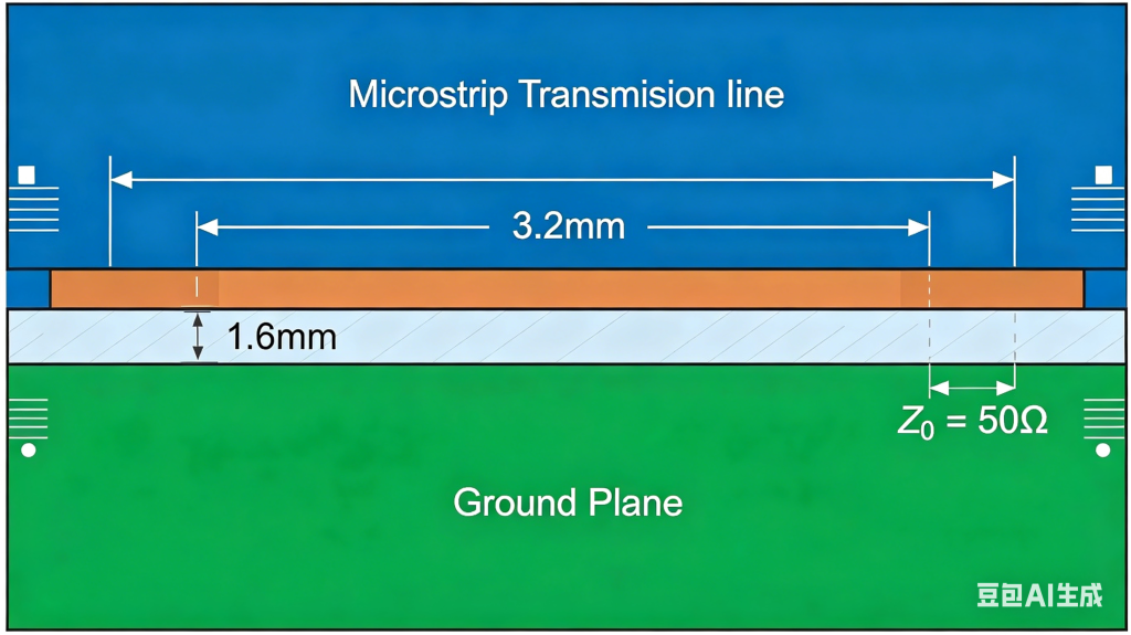
Transmission Line Theory and Characteristic Impedance Control
High-Speed PCB Design begins with transmission line theory. Every trace behaves as a transmission line at high frequencies. The three most authoritative sources agree that controlling characteristic impedance (Z₀) is paramount. For standard interfaces like DDR, PCIe, and USB, target Z₀ = 50Ω single-ended or 90-100Ω differential. Achieve this by precisely controlling trace width, dielectric thickness, and dielectric constant (Dk). Use field solvers such as Polar Si9000 or Ansys Q3D to calculate Z₀ before layout, not after. Avoid impedance discontinuities from abrupt trace width changes, layer transitions, or reference plane gaps. Each discontinuity creates reflections that degrade signal quality. The rule of thumb: keep discontinuities shorter than 1/10th of the signal rise time. Stubs and branches cause resonances and reflections; for multi-drop buses, use daisy-chain or fly-by topology, avoiding T-junctions. In DDR4/5, fly-by topology is mandatory for clock and address/command signals.
Loss Mechanisms and Mitigation in High-Speed PCB Design
High-Speed PCB Design must address three primary loss types. Ohmic loss (skin effect) concentrates current on the conductor surface at high frequencies; use smoother copper (RTF or VLP) and wider traces to reduce resistance. For critical nets, consider copper foil with low profile (e.g., 1 oz or 2 oz, noting thicker copper increases capacitance). Dielectric loss (dissipation factor Df) is significant at multi-GHz frequencies; FR-4 has high Df (~0.02 at 1 GHz), so for 10+ Gbps designs, use low-loss materials like Rogers 4003C, Megtron 6, or Isola IS415. Always specify Df and Dk tolerance from your manufacturer. Surface roughness increases loss; specify very low profile (VLP) or reverse treated foil for high-speed layers.
Crosstalk and Coupling Control
Crosstalk occurs when an aggressor signal induces voltage on a victim trace. The 3W rule for microstrip traces spaces them at least 3 times the trace width edge-to-edge to reduce crosstalk below 5%. For stripline inner layers, 2W is often sufficient. Reference plane integrity is critical: never route a high-speed trace over a split in the reference plane, as return current is forced around the gap, creating large loop areas that radiate noise and increase crosstalk. For ultra-sensitive signals like analog or clock, place a grounded guard trace between aggressor and victim, stitching it to the ground plane with vias every λ/10 (wavelength/10).
Power Integrity in High-Speed PCB Design
Power Distribution Network (PDN) and Target Impedance
Power integrity is as critical as signal integrity in High-Speed PCB Design. The goal is to maintain stable voltage with minimal ripple (typically <5% of nominal voltage). Calculate target impedance (Z_target) using: Z_target = (V_rail * Ripple%) / I_transient. For a 1.2V rail with 5% ripple and a 10A transient, Z_target = 6 mΩ. Decoupling capacitor strategy alone cannot achieve flat impedance below 10 mΩ; use a hierarchy: bulk capacitors (10-100 µF) for low-frequency (<1 MHz), ceramic MLCCs (0.1-10 µF) for mid-range (1-100 MHz), and PCB plane capacitance for high frequencies (>100 MHz). Power and ground planes act as a capacitor; use thin dielectric between them (2-4 mils) to maximize capacitance, often more effective than many small capacitors.
PDN Simulation and Measurement Techniques
Frequency-domain simulation uses SPICE or EM simulators (Ansys SIwave, Cadence Sigrity) to plot PDN impedance vs. frequency; the curve must stay below Z_target across the entire frequency range of interest (DC to clock frequency). Time-domain simulation evaluates voltage ripple under worst-case transient loads (e.g., DDR read/write bursts), revealing if the PDN handles sudden current changes without drooping. Measurement uses a vector network analyzer (VNA) with a 2-port shunt-through technique to measure PDN impedance on a prototype, or a high-bandwidth oscilloscope with a low-inductance probe to measure ripple at IC pins.
Via Modeling for High-Speed PCB Design
Via Structure and Parasitic Effects
Vias are often the weakest link in High-Speed PCB Design. A via introduces inductance, capacitance, and resistance that can ruin signal quality. Via inductance (L_via) is dominated by loop area; approximate formula: L_via = 5.08 * h * [ln(4h/d) + 1] (nH), where h is via length (mm) and d is via diameter (mm). Minimize L_via by using shorter vias (avoid long stubs), smaller anti-pads, and multiple ground vias nearby. Via capacitance (C_via) comes from pad-to-plane and barrel-to-plane coupling; approximate formula: C_via = 1.41 * ε_r * D1 * D2 / (D2 – D1) (pF), where D1 is pad diameter and D2 is anti-pad diameter. Reduce C_via by increasing anti-pad clearance or using back-drilled vias to remove unused stub. Via resistance at DC is low, but skin effect increases resistance at high frequencies; use larger barrels (12-18 mil finished diameter) for high-current vias.
Via Stub Effects and Mitigation Strategies
A via stub is the unused portion of a via barrel beyond the target layer, acting as a resonant cavity causing insertion loss peaks at frequencies where stub length equals λ/4. Back-drilling is the most effective mitigation; drill out the stub from the bottom side after plating, specifying back-drill depth tolerance (typically ±5 mils). For 25 Gbps+ designs, back-drilling is mandatory. Blind/buried vias use laser-drilled microvias (4-6 mil diameter) to connect adjacent layers without stubs, eliminating the stub entirely but increasing cost. Via-in-pad for BGA packages places the via directly under the pad (filled and plated over), reducing loop inductance but requiring careful manufacturing (conductive epoxy fill or copper plug).
Differential Via Design Considerations
For differential pairs (USB, HDMI, PCIe), vias must be designed as a pair. Symmetry is critical: both vias must have identical geometry (barrel diameter, anti-pad, stub length); asymmetry causes common-mode noise. Place 2-4 ground vias symmetrically around the differential via pair (e.g., at 45° or 90° positions) to provide low-inductance return paths and reduce mode conversion. Use an elongated anti-pad (dog-bone shape) to reduce capacitance while maintaining controlled impedance through the via. Simulate differential impedance (Z_diff) through the via transition; it should match trace impedance (e.g., 100Ω).
SI/PI Co-Simulation and Practical Workflow
The Co-Simulation Approach for High-Speed PCB Design
Separate SI and PI simulations can miss interactions; for example, a noisy PDN can inject jitter into a clock signal. Use tools that couple SI and PI (Ansys HFSS with SIwave, or Cadence Sigrity with PowerDC). Simulate the entire channel (driver → trace → via → receiver) with a realistic PDN model. Use IBIS (I/O Buffer Information Specification) models for drivers and receivers, including output impedance, rise/fall times, and power supply sensitivity. Ensure your model version matches actual silicon. After simulation, check the eye diagram at the receiver. Key metrics: eye height (≥ 200 mV for 1.2V logic), eye width (≥ 0.7 UI), and jitter (peak-to-peak < 0.2 UI).
Design for Manufacturability (DFM) Considerations
Work with your PCB manufacturer early. Specify a stack-up that meets impedance, plane capacitance, and layer count needs. Include a prepreg-core-prepreg structure for controlled impedance. Via tolerances (e.g., ±2 mils on via diameter, ±1 mil on anti-pad) affect parasitics; run Monte Carlo simulation in your EM tool to ensure design robustness. For high-reliability designs, specify materials with tight Dk tolerance (e.g., ±2%) and low moisture absorption; avoid generic FR-4; use materials with a datasheet specifying Dk and Df at your operating frequency.
Case Study: 25 Gbps NRZ Channel in High-Speed PCB Design
Problem Statement
Design a 25 Gbps NRZ channel from a SerDes to a connector over a 6-inch trace, using a 4-layer PCB (top: signal, GND, PWR, bottom: signal). Target Z₀ = 50Ω, PDN Z_target < 10 mΩ.
Solution Steps
- Stack-Up: Use 0.5 oz copper on outer layers, 1 oz on inner. Core thickness: 4 mils between top and GND (for microstrip), 40 mils between GND and PWR (for plane capacitance), 4 mils between PWR and bottom.
- Trace Design: Width = 8 mils (microstrip on top). Use 45° bends, no right angles.
- Via Design: Use a 12-mil finished barrel via from top to bottom. Back-drill to remove stub from bottom layer. Place two 10-mil ground vias 20 mils away from the signal via (center-to-center). Anti-pad diameter = 28 mils.
- PDN: Add 10x 0.1 µF capacitors near the SerDes. Use 2x 10 µF bulk capacitors. Simulate PDN impedance; verify it stays below 10 mΩ.
- Simulation: Run SI simulation with IBIS model. Eye diagram shows eye height = 350 mV, eye width = 0.75 UI, jitter = 0.12 UI. Pass.
Key Lessons
- Back-drilling reduced insertion loss by 3 dB at 12.5 GHz.
- Two ground vias reduced via inductance by 40% compared to a single via.
- PDN simulation revealed a resonance at 150 MHz; adding a 1 µF capacitor dampened it.
Comparison: Our High-Speed PCB Design Capabilities vs. Industry Standards
| Parameter | Industry Standard | Our High-Speed PCB Design Service |
|---|---|---|
| Impedance Tolerance | ±10% | ±5% (verified by TDR) |
| Back-Drilling Depth Tolerance | ±10 mils | ±5 mils |
| Low-Loss Material Options | Limited to FR-4 | Rogers, Megtron 6, Isola IS415 |
| Via-in-Pad Capability | Not standard | Copper-filled and plated |
| SI/PI Co-Simulation Support | Basic | Full Ansys/Cadence workflow |
Glossary of Key Terms in High-Speed PCB Design
- Signal Integrity (SI): The quality of an electrical signal as it travels from driver to receiver, affected by reflections, crosstalk, and loss.
- Power Integrity (PI): The stability of voltage and current supplied to ICs, managed through PDN design and decoupling.
- Via Modeling: The analysis of via parasitics (inductance, capacitance, resistance) to minimize signal degradation.
- Characteristic Impedance (Z₀): The impedance a transmission line presents to a propagating signal; typically 50Ω for single-ended traces.
- Back-Drilling: A process to remove unused via stubs, reducing resonances and insertion loss at high frequencies.
- Eye Diagram: A graphical representation of signal quality, showing eye height, eye width, and jitter.
- IBIS Model: I/O Buffer Information Specification model used for simulating driver/receiver behavior.
- Dissipation Factor (Df): A measure of dielectric loss; lower Df indicates better high-frequency performance.
Frequently Asked Questions (FAQ) About High-Speed PCB Design
What is High-Speed PCB Design?
High-Speed PCB Design refers to the practice of designing printed circuit boards for signals with rise times fast enough that transmission line effects (reflections, crosstalk, loss) become significant. It requires careful impedance control, via modeling, and power integrity analysis.
Why is via modeling important in High-Speed PCB Design?
Via modeling is critical because vias introduce parasitic inductance and capacitance that can cause signal reflections, jitter, and increased loss. Proper via modeling ensures that via transitions do not degrade signal quality, especially at multi-GHz data rates.
How do I choose materials for High-Speed PCB Design?
Choose materials with low dissipation factor (Df) and tight dielectric constant (Dk) tolerance for high-speed layers. For designs above 10 Gbps, use Rogers 4003C, Megtron 6, or Isola IS415. Always verify Dk and Df at your operating frequency with the manufacturer.
What is the difference between SI and PI in High-Speed PCB Design?
Signal Integrity (SI) focuses on the quality of signals as they travel through traces and vias, while Power Integrity (PI) ensures stable voltage and current delivery to ICs. Both are interdependent; a noisy PDN can degrade SI, and poor SI can cause power supply noise.
What tools are used for SI/PI co-simulation in High-Speed PCB Design?
Industry-standard tools include Ansys HFSS, SIwave, and Cadence Sigrity with PowerDC. These tools allow coupled simulation of signal and power domains, providing accurate eye diagrams and PDN impedance plots.