Embedded Component PCB technology, integrating capacitors and resistors directly into inner layers, revolutionizes miniaturization and signal integrity for high-performance electronics. This definitive guide covers everything from planar capacitor layers to embedded resistor manufacturing, design best practices, and future trends—empowering engineers to leverage this advanced PCB solution for compact, reliable, and high-speed designs.
What Are Embedded Component PCBs? Core Concepts & Definitions
The Fundamental Principle
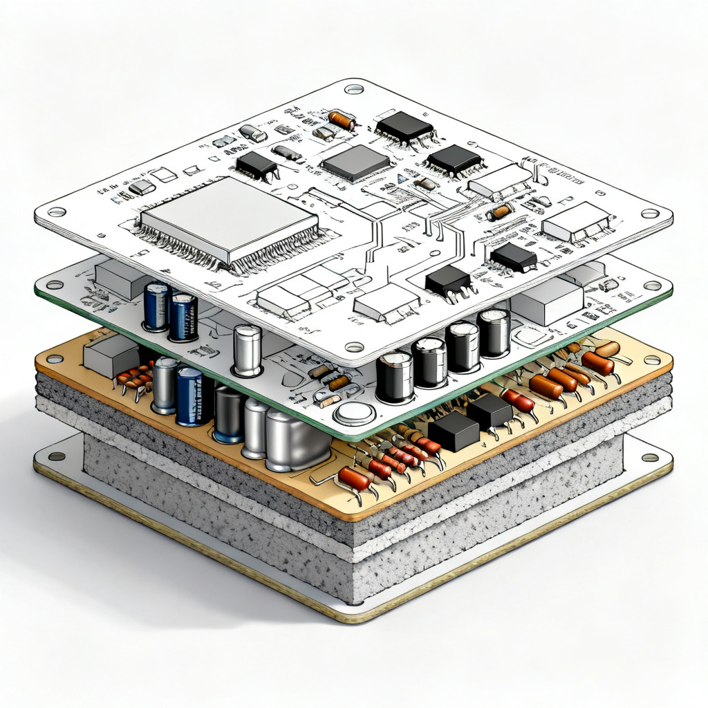
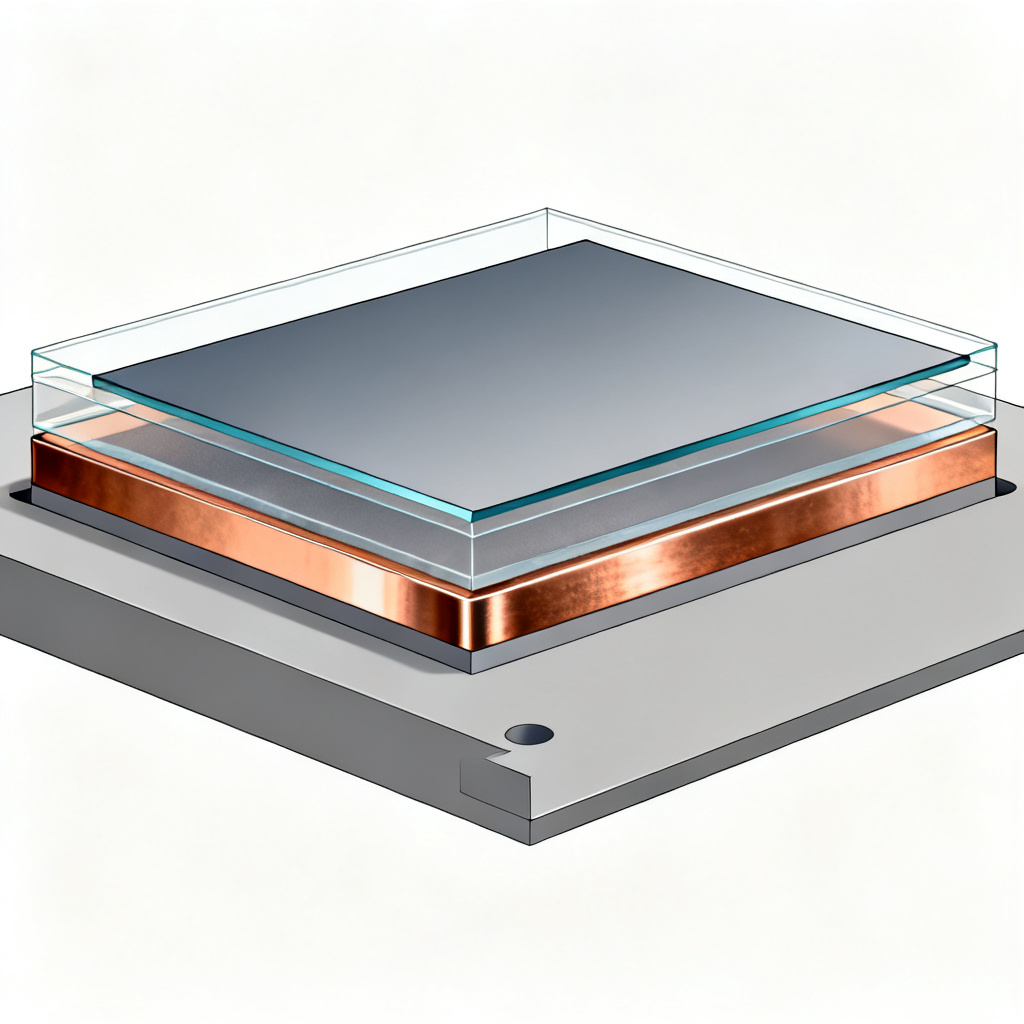
Embedded Component PCB technology integrates passive or active electronic components into the internal layers of a PCB substrate, rather than mounting them on outer surfaces. For capacitors and resistors, this means they are manufactured as part of the PCB laminate itself—either as discrete pre-fabricated components placed into cavities or as planar layers of resistive or dielectric material that are etched or deposited to form specific values.
Key Distinction: Embedded vs. Buried vs. Surface Mount
Surface Mount (SMT) involves components soldered onto outer copper pads. Buried components are passive components placed within inner layers but require separate component placement. Embedded components are fully integrated into the PCB structure—capacitors use thin, high-dielectric-constant material as a core layer, while resistors involve depositing or laminating resistive material (like nickel-phosphorus) that is laser-trimmed or etched for precise values. The component becomes an intrinsic part of the PCB’s physical structure.
Why Embed? The Primary Drivers
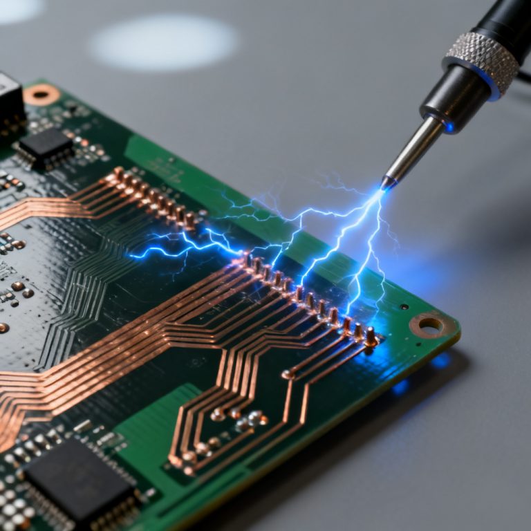
Miniaturization frees surface area or reduces overall board size for compact devices like smartphones, wearables, medical implants, and IoT sensors. Improved signal integrity results from shorter interconnects between embedded components and active ICs, reducing parasitic inductance and capacitance for cleaner signals and better high-frequency performance. Enhanced thermal management allows placement closer to thermal vias or heat sinks for improved heat dissipation. Increased reliability protects components from mechanical stress, vibration, and environmental contaminants, with no solder joints to fail. Design freedom enables placement in impossible locations for SMT, such as directly under a BGA package.
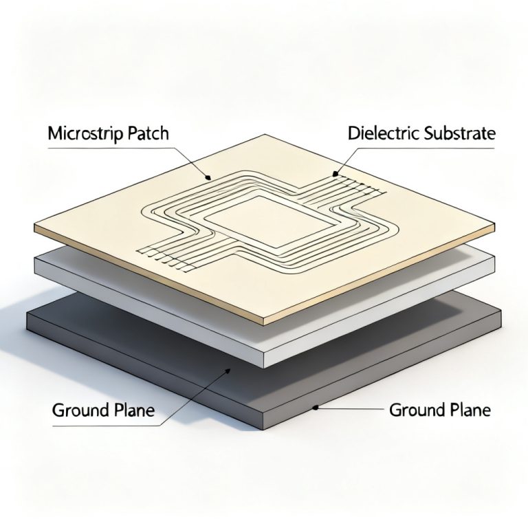
Embedded Capacitors Inside PCB Layers: Technology & Performance
The Technology: Planar Capacitor Layers
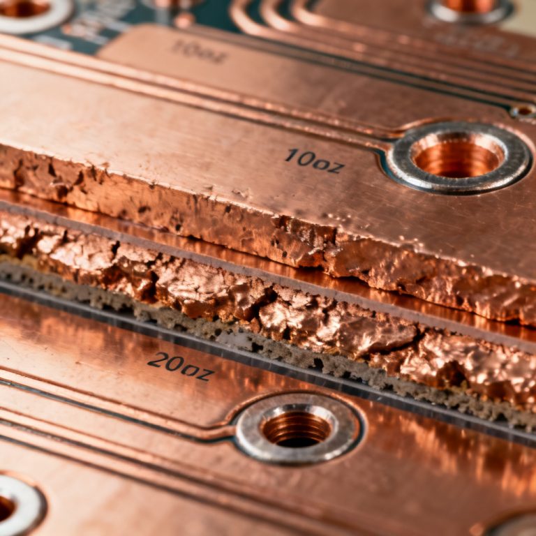
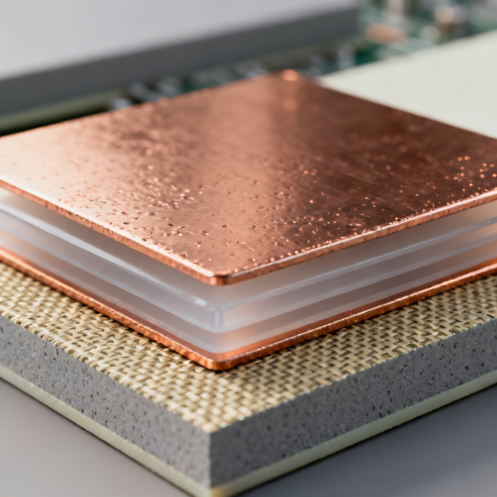
The most common method for embedding capacitors uses planar capacitor layers, replacing a standard core layer (e.g., FR4) with a specialized laminate having a very high dielectric constant (Dk). This thin, high-Dk material is sandwiched between two copper foil layers, effectively creating a large, distributed capacitor. Material options include ceramic-filled polymer laminates with Dk values of 10–30, compatible with standard PCB manufacturing, and thin-film dielectrics like barium titanate (BaTiO3) or lead zirconate titanate (PZT) sputtered or screen-printed for ultra-thin layers with capacitance density up to 10–100 nF/cm². The entire layer acts as a capacitor; by etching patterns in the copper layers, multiple discrete capacitors are created—a section of copper on one side of the dielectric becomes one plate, and the corresponding section on the other side becomes the other plate. Capacitance value is determined by plate area, dielectric constant, and dielectric thickness.
Discrete Embedded Capacitors
Pre-manufactured discrete capacitors (often ultra-thin, 0.1–0.4 mm thick) can be placed into cavities or recesses in inner layers, then laminated into the stack-up. This approach allows precise capacitance values for specific, non-standard requirements.
Performance Advantages of Embedded Capacitors
Ultra-low parasitic inductance (ESL) is achieved because the capacitor is built into the PCB, making connections to the power plane extremely short—ESL can be reduced by a factor of 10–100 compared to SMT capacitors. Low equivalent series resistance (ESR) results from the direct copper-to-dielectric interface. Excellent high-frequency decoupling makes embedded capacitors ideal for bypassing noise at GHz frequencies where SMT capacitors become ineffective due to parasitic inductance. Space savings are significant—a single planar capacitor layer can replace dozens of SMT decoupling capacitors.
Design Considerations for Embedded Capacitors
Capacitance density versus voltage rating requires balancing higher density with thinner dielectrics that reduce voltage ratings. Material selection must match the Dk and dissipation factor (Df) to the application’s frequency and temperature requirements. Manufacturing tolerances for planar capacitors are wider (e.g., ±10–20%) than precision SMT capacitors, so discrete embedded capacitors or trimming may be needed for critical timing circuits. Thermal expansion compatibility between the dielectric material’s coefficient of thermal expansion (CTE) and surrounding FR4 or other laminate layers is essential to prevent delamination.
Embedded Resistors Inside PCB Layers: Technology & Performance
The Technology: Planar Resistor Layers
Embedded resistors are most commonly implemented using planar resistor layers. A thin layer of resistive material—typically a metal alloy like nickel-phosphorus (NiP) or a ceramic-filled polymer—is laminated onto a copper foil. This “resistor foil” is processed like a standard copper layer but with an additional etching step to define the resistive elements. Material options include NiP, the most mature and widely used material offering good stability, low TCR (Temperature Coefficient of Resistance), and laser-trimmability for tight tolerances; tantalum nitride (TaN) for high-precision applications requiring very low TCR and high reliability; and carbon-filled polymers for lower cost but wider tolerances and higher TCR, suitable for less critical applications. The resistive layer is typically sandwiched between two copper layers; copper is etched to create contact pads at the ends of the resistor, and the resistor itself is the exposed resistive material between these pads. Resistance value is determined by length, width, and sheet resistance (ohms per square) of the material.
Discrete Embedded Resistors
Discrete resistor chips (e.g., 0402 or 0201 size) can be placed into cavities, though this is less common than planar resistors. It is useful for high-power resistors or specific values difficult to achieve with planar technology.
Performance Advantages of Embedded Resistors
Elimination of solder joints means no cold joints, solder bridging, or reliability issues related to thermal cycling. Improved high-frequency performance comes from extremely short connections to active devices, minimizing parasitic inductance and capacitance—ideal for RF and high-speed digital circuits. Reduced board size results from replacing dozens of SMT resistors. Lower assembly cost comes from fewer components to place and solder, reducing pick-and-place time and potential defects. Better thermal management is achieved because the resistive material is in direct contact with the PCB substrate, which acts as a heat sink.
Design Considerations for Embedded Resistors
Power dissipation is limited (typically 0.05–0.25 W per resistor) due to the insulating nature of the surrounding laminate; heat must be conducted away through PCB layers. Tolerance and trimming: as-deposited planar resistors have tolerances of ±10–20%, but laser trimming can achieve ±0.5% or better, though this adds cost and process time. TCR (Temperature Coefficient of Resistance) for NiP is approximately ±50–100 ppm/°C, acceptable for most applications but not for precision analog circuits. Layout and routing must ensure the resistor is placed where the resistive material will not be damaged during subsequent lamination or drilling steps.
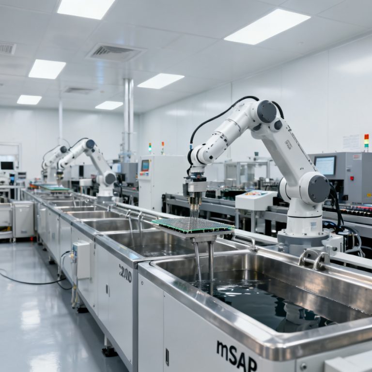
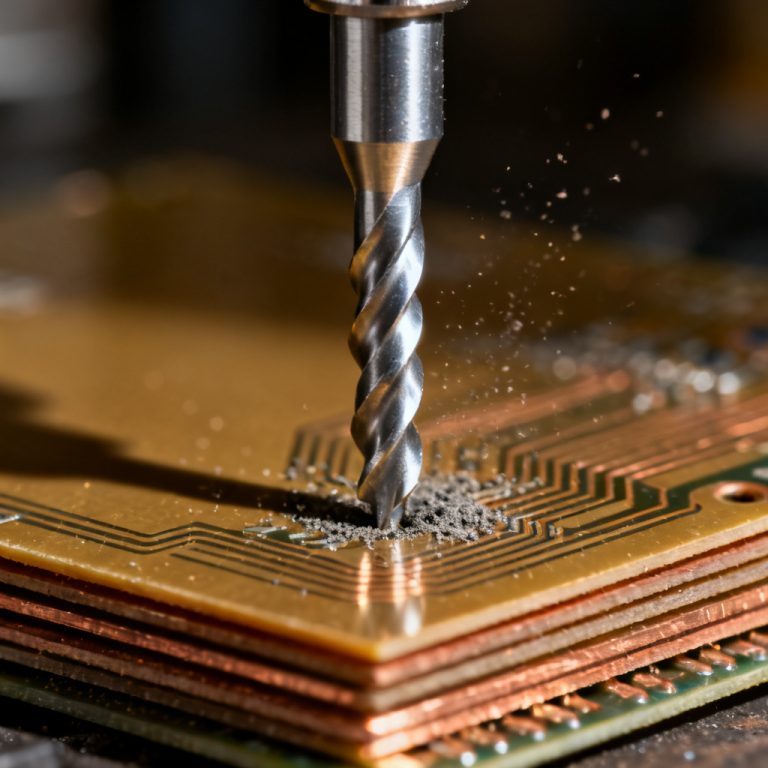
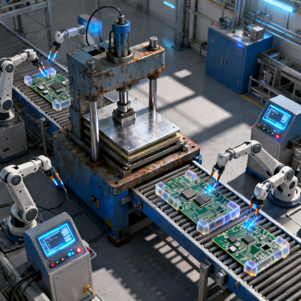
Manufacturing Process for Embedded Component PCBs
Step-by-Step Process
- Core Preparation: Start with a standard core or specialized embedded component core (e.g., high-Dk laminate for capacitors or NiP-coated foil for resistors).
- Inner Layer Imaging & Etching: For planar components, pattern copper layers using standard photolithography and etching to define capacitor plates or resistor contact pads.
- Resistive Layer Processing (for Resistors): After etching copper, leave exposed resistive material as-is for the resistor body or selectively etch it away to isolate individual resistors.
- Laser Trimming (Optional): Precisely cut resistive material using a laser to adjust length-to-width ratio for tight tolerances.
- Lamination: Stack inner layers, including embedded component layers, with prepreg (bonding sheets) and copper foil, then laminate under high heat and pressure to form a monolithic board.
- Drilling & Plating: Drill holes through the board; carefully place vias to connect component contact pads to other layers without damaging the component.
- Outer Layer Processing: Image, etch, and plate outer layers as usual.
- Solder Mask & Surface Finish: Apply to outer layers.
- Testing: Use electrical testing (e.g., flying probe) to verify resistance and capacitance values of embedded components.
Key Challenges in Manufacturing
Material compatibility requires embedded component materials (dielectrics, resistive films) to be compatible with thermal and chemical processes of PCB manufacturing (e.g., lamination temperature, etching chemistries). Registration demands very tight tolerances (typically ±10–20 microns) to align embedded components with the rest of the PCB layers. Yield can be lower if the process is not carefully controlled, and defects in embedded components are difficult to repair. Cost increases due to specialized materials and additional processing steps (e.g., laser trimming), but this can be offset by savings in assembly cost and board size.
Applications & Use Cases for Embedded Component PCBs
High-Speed Digital & RF Circuits
Smartphones and tablets use embedded capacitors for decoupling high-speed processors and RF transceivers, improving signal integrity and reducing board size. Base stations and networking equipment use embedded resistors and capacitors in impedance matching networks and filter circuits. 5G and millimeter-wave systems benefit from low parasitic inductance critical for maintaining signal quality at GHz frequencies.
Power Electronics
DC-DC converters use embedded capacitors as input/output filters, reducing ripple and improving transient response. Power management ICs (PMICs) benefit from embedding decoupling capacitors directly under the package to reduce loop inductance.
Medical Devices
Implantable devices (pacemakers, neurostimulators) require high reliability and small size from embedded components for long-term, implantable electronics. Hearing aids and wearable sensors prioritize miniaturization.
Automotive Electronics
ADAS (Advanced Driver-Assistance Systems) radar and lidar modules benefit from high-frequency performance. Engine control units (ECUs) rely on ruggedness and reliability for harsh automotive environments.
Aerospace & Defense
Satellite and avionics applications require ability to withstand vibration, shock, and extreme temperatures, making embedded component PCBs ideal for high-reliability applications.
Comparison: Embedded Components vs. Traditional SMT
| Feature | Embedded Component PCB | Traditional SMT PCB |
|---|---|---|
| Board Size | Significantly smaller (30–50% reduction possible) | Larger, limited by component footprint |
| Signal Integrity | Excellent (low parasitic inductance/capacitance) | Good, but limited by long traces and component leads |
| Reliability | Higher (no solder joints, protected from environment) | Lower (solder joints are failure points) |
| Assembly Cost | Lower (fewer components to place) | Higher (more pick-and-place steps) |
| PCB Fabrication Cost | Higher (special materials, additional processes) | Lower (standard materials, simpler process) |
| Design Complexity | Higher (requires specialized CAD tools and simulation) | Lower (standard layout rules) |
| Repairability | Very difficult (components are buried) | Easier (components are accessible) |
| Power Handling | Limited (for resistors) | Higher (for discrete resistors) |
| Tolerance | Wider (for planar components) | Tighter (for discrete SMT components) |
Design Guidelines & Best Practices
For Embedded Capacitors
Use a dedicated power plane layer to embed the capacitor layer as a power plane for maximum decoupling effectiveness. Minimize via distance by placing vias connecting the capacitor plate to the IC’s power pin as close as possible. Simulate the stack-up using electromagnetic simulation tools to model impedance and resonance of the embedded capacitor layer. Consider the dielectric material’s frequency response, as Dk and Df can vary with frequency; choose a material stable in your operating band.
For Embedded Resistors
Keep resistor values within a practical range of typically 10 ohms to 1 Mohm for planar resistors; very low or very high values are difficult to achieve. Avoid placing resistors near high-stress areas such as mounting holes or areas subject to bending. Use thermal vias for power resistors—if a resistor needs to dissipate more than 0.1 W, place thermal vias under or adjacent to it. Laser trimming is a design choice: if you need ±1% tolerance, plan for laser trimming; if ±10% is acceptable, skip it to save cost.
General Best Practices
Work closely with your PCB manufacturer, as embedded component technology requires close collaboration for advice on material availability, process capabilities, and design rules. Use specialized EDA tools like Cadence Allegro, Altium Designer (with appropriate extensions), or Zuken, as standard PCB design software may not support embedded components. Create a separate design rule set defining specific rules for embedded component layers, including clearance, minimum width, and via placement. Prototype early given the higher cost and complexity, building a prototype to verify the design before moving to production.
The Future of Embedded Component Technology
The trend is clear: more integration, higher density, and lower cost. Future developments include active component embedding, where embedding active devices like ICs and transistors inside the PCB is already in use (e.g., in some smartphones) and will become more widespread. 3D-printed electronics combine additive manufacturing with embedded component technology for truly flexible and custom-shaped circuits. Advanced materials include new high-Dk dielectrics with even lower loss (Df) and better thermal conductivity. Automated design tools using AI-driven optimization automatically optimize placement and value of embedded components for maximum performance and minimum cost. Embedded sensors integrate temperature, pressure, and humidity sensors directly into the PCB for smart IoT devices.
Frequently Asked Questions (FAQ)
What is an Embedded Component PCB?
An Embedded Component PCB integrates passive components like capacitors and resistors directly into the inner layers of the PCB substrate, rather than mounting them on the surface. This technology is used to achieve miniaturization, improved signal integrity, and higher reliability in compact electronic devices.
How are capacitors embedded inside PCB layers?
Capacitors are embedded using planar capacitor layers, where a thin, high-dielectric-constant material is sandwiched between copper foils. This creates distributed capacitance, and by etching patterns, discrete capacitors are formed. Discrete capacitors can also be placed into cavities for precise values.
How are resistors embedded inside PCB layers?
Resistors are embedded using planar resistor layers, where a resistive material like nickel-phosphorus is laminated onto a copper foil and etched to define resistive elements. Laser trimming can achieve tight tolerances. Discrete resistor chips can also be placed into cavities for high-power or specific values.
What are the main advantages of embedded component PCBs over traditional SMT?
Embedded component PCBs offer smaller board size (30–50% reduction), better signal integrity due to shorter interconnects, higher reliability with no solder joints, lower assembly cost from fewer components, and enhanced thermal management.
What applications benefit most from embedded capacitors and resistors?
High-speed digital and RF circuits (smartphones, 5G, base stations), power electronics (DC-DC converters), medical devices (implantables), automotive electronics (ADAS), and aerospace/defense (satellites) all benefit from the miniaturization, signal integrity, and reliability of embedded component PCBs.
Conclusion: Is Embedded Component PCB Right for Your Project?
Embedded Component PCB technology—specifically the integration of capacitors and resistors inside the layers—is a powerful tool for engineers seeking to push the boundaries of miniaturization, performance, and reliability. While it comes with higher fabrication costs and design complexity, the benefits in terms of space savings, signal integrity, and assembly cost reduction can be transformative, especially for high-volume, high-performance applications.
When to choose embedded components: You need to reduce board size by 30% or more. Your design operates at GHz frequencies where parasitic inductance is a problem. You are assembling thousands of boards and want to reduce pick-and-place costs. Reliability is critical (medical, aerospace, automotive).
When to stick with SMT: Your budget is extremely tight. You need high-power resistors (>0.25 W). Your design requires frequent prototyping or rework. You are working with very low volumes.
By understanding the principles, materials, and processes outlined in this pillar page, you can make an informed decision and leverage the full potential of embedded component technology to create the next generation of electronic products.
Need expert guidance on designing or manufacturing Embedded Component PCBs for your next project? Contact our team today for a free consultation and stack-up analysis.